Home > Press > John Hopkins University sends students to imec for summer research on biomedical devices and jointly presents first results on ‘nanoscale origami’
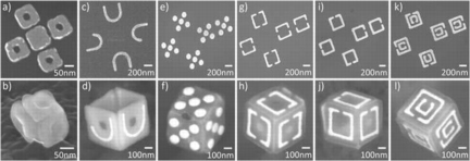 |
| Figure JHU_1: Scanning electron microscopy (SEM) images of the patterns (a-hollow squares; c-alphabet; d-dice-like; e-f-g-SSRs) and folded cubes. |
Abstract:
This summer, imec welcomed 4 students from John Hopkins University (JHU), a world-class university in Baltimore, US, for a research internship of 10 weeks in the field of bioelectronics. These internships coincide with the announcement of a scientific story on nanoscale origami that has resulted from the internship of the first JHU visiting student in the summer of 2009 with a follow-on program last year. In this work, an approach is presented that allows generating precisely patterned polyhedral nanostructures, envisaged for optical and biosensing applications.
John Hopkins University sends students to imec for summer research on biomedical devices and jointly presents first results on ‘nanoscale origami’
Leuven, Belgium and Baltimore, MD | Posted on August 26th, 2011JHU-imec exchange project
The students - both graduate and undergraduate - learn to design, fabricate and test a wide range of biomedical devices at imec. One of the internships is part of a collaboration that is ongoing for two years. In January 2012, the first student from imec will have the unique opportunity to work with researchers from the Institute for Nanobiotechnology at John Hopkins University. The overall exchange project is enabled by the International Research Experience for Students (IRES) program, which is funded by the National Science Foundation. These internships are very valuable as they contribute to the learning experience of the students and enrich the research activities of both imec and JHU. Besides this project, imec has an agreement with Olin College, US, to exchange students for intensive internships at imec or Olin, and has plans to extend its collaboration with other top universities and institutes in the US.
You can view here [link naar filmpje] how this year's students experience their internship at imec.
In addition, we present a scientific story on ‘nanoscale origami' that has resulted from the internship of the first JHU visiting student, Michael Keung, who worked at imec in 2009 and 2010. The work has been published in a special issue of the journal Small, vol. 7, n°14, July 2011, and an image from the paper was selected as the inside cover image. The paper results from collaboration between imec and David Gracias' group at John Hopkins University. Michael Keung has since completed his M.S. in Engineering.
‘Nanoscale origami' enables the creation of 3D nanostructured devices for optics and biosensing
An origami-inspired approach is presented that allows generating precisely patterned polyhedral nanostructures. The method is based on the nanoscale self-folding of samples that have been patterned using electron-beam (e-beam) lithography. The nanoscale origami approach can greatly augment the capabilities of miniaturized optical devices and can be used for applications in biosensing. The technique has been demonstrated by the creation of structures with optically active split-ring resonator (SRR) patterns.
The novel approach allows precisely patterning optical or electronic elements in two dimensions and subsequently folding them up into three dimensions - just like the ancient Japanese art of paper folding. Transforming 2D patterns into 3D patterns presents a major advantage as compared to existing 3D nanostructures which have only very limited surface patterns. The method allows the creation of various polyhedral nanostructures with a versatility in the types of patterns, and are envisaged for optical and biosensing applications.
The overall process flow consists of first patterning in 2D the optically or electronically relevant features by using e-beam lithography and lift-off processes. After patterning, subsequent steps of e-beam lithography are used to define panels and hinges. Next, the structures are released from the substrate by using plasma etching of the underlying Si substrate. During etching, the heat generated by the exothermic etching process causes grain coalescence or reflow of the hinges. The hinges act as self-folds by generating a torque to rotate panels and create the 3D nanostructures. The fold angle can be controlled by tuning the plasma processing conditions. Sn was used as the hinge material and either Ni or Al2O3 was used as the panel material.
With this technique, geometric shapes, alphabets and three types of SRRs (with cube sizes 100nm and 500nm) have been patterned within a single Au layer. Patterns of Au SRRs are especially relevant for 3D optics. Reflection spectra of a folded nanocube with a single SRR patterned on each of the six faces was successfully collected by using infrared excitation. The expected polarization dependence is clearly observed. The researchers demonstrated another interesting functionality that consists in generating a unique plasmonic barcode on all faces. This allows seeing the orientation of the cube by optical probing and can be used as an optical gyroscope with plenty of opportunities for bioresearch. In the future, further experimentation is required to extend the nanoscale origami approach to other material combinations.
####
About IMEC
Imec performs world-leading research in nano-electronics and nano-technology. Its staff of more than 1,900 people includes over 500 industrial residents and guest researchers. Imec’s research is applied in better healthcare, smart electronics, sustainable energy, and safer transport.
For more information, please click here
Contacts:
Barbara Kalkis
Maestro Marketing & PR
Copyright © IMEC
If you have a comment, please Contact us.Issuers of news releases, not 7th Wave, Inc. or Nanotechnology Now, are solely responsible for the accuracy of the content.
Bookmark:


| Related News Press |
News and information
![]() Simulating magnetization in a Heisenberg quantum spin chain April 5th, 2024
Simulating magnetization in a Heisenberg quantum spin chain April 5th, 2024
![]() NRL charters Navy’s quantum inertial navigation path to reduce drift April 5th, 2024
NRL charters Navy’s quantum inertial navigation path to reduce drift April 5th, 2024
![]() Discovery points path to flash-like memory for storing qubits: Rice find could hasten development of nonvolatile quantum memory April 5th, 2024
Discovery points path to flash-like memory for storing qubits: Rice find could hasten development of nonvolatile quantum memory April 5th, 2024
Govt.-Legislation/Regulation/Funding/Policy
![]() NRL charters Navy’s quantum inertial navigation path to reduce drift April 5th, 2024
NRL charters Navy’s quantum inertial navigation path to reduce drift April 5th, 2024
![]() Discovery points path to flash-like memory for storing qubits: Rice find could hasten development of nonvolatile quantum memory April 5th, 2024
Discovery points path to flash-like memory for storing qubits: Rice find could hasten development of nonvolatile quantum memory April 5th, 2024
![]() Chemical reactions can scramble quantum information as well as black holes April 5th, 2024
Chemical reactions can scramble quantum information as well as black holes April 5th, 2024
Academic/Education
![]() Rice University launches Rice Synthetic Biology Institute to improve lives January 12th, 2024
Rice University launches Rice Synthetic Biology Institute to improve lives January 12th, 2024
![]() Multi-institution, $4.6 million NSF grant to fund nanotechnology training September 9th, 2022
Multi-institution, $4.6 million NSF grant to fund nanotechnology training September 9th, 2022
Nanomedicine
![]() New micromaterial releases nanoparticles that selectively destroy cancer cells April 5th, 2024
New micromaterial releases nanoparticles that selectively destroy cancer cells April 5th, 2024
![]() Good as gold - improving infectious disease testing with gold nanoparticles April 5th, 2024
Good as gold - improving infectious disease testing with gold nanoparticles April 5th, 2024
![]() Researchers develop artificial building blocks of life March 8th, 2024
Researchers develop artificial building blocks of life March 8th, 2024
Announcements
![]() NRL charters Navy’s quantum inertial navigation path to reduce drift April 5th, 2024
NRL charters Navy’s quantum inertial navigation path to reduce drift April 5th, 2024
![]() Discovery points path to flash-like memory for storing qubits: Rice find could hasten development of nonvolatile quantum memory April 5th, 2024
Discovery points path to flash-like memory for storing qubits: Rice find could hasten development of nonvolatile quantum memory April 5th, 2024
Nanobiotechnology
![]() New micromaterial releases nanoparticles that selectively destroy cancer cells April 5th, 2024
New micromaterial releases nanoparticles that selectively destroy cancer cells April 5th, 2024
![]() Good as gold - improving infectious disease testing with gold nanoparticles April 5th, 2024
Good as gold - improving infectious disease testing with gold nanoparticles April 5th, 2024
![]() Researchers develop artificial building blocks of life March 8th, 2024
Researchers develop artificial building blocks of life March 8th, 2024
|
|
||
|
|
||
| The latest news from around the world, FREE | ||
|
|
||
|
|
||
| Premium Products | ||
|
|
||
|
Only the news you want to read!
Learn More |
||
|
|
||
|
Full-service, expert consulting
Learn More |
||
|
|
||