Home > Press > Electrons and Lattice Vibrations—A Strong Team in the Nano World
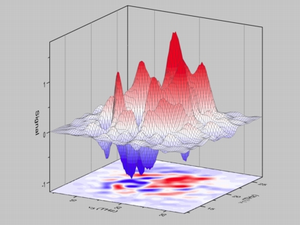 |
| Measured two-dimensional spectrum. Without the interaction of the electron with lattice vibrations there would be no signal in the range shown. |
Abstract:
Using a newly developed type of spectroscopy, Berlin researchers have shown that electrons in a semiconductor are best described as a cloud with a size of a few nanometer (one nanometer is one billionth of one meter). The cloud size is determined by the interaction of the electron with vibrations in the crystal lattice.
Electrons and Lattice Vibrations—A Strong Team in the Nano World
Berlin, Germany | Posted on August 6th, 2011Semiconductor electronics generates, controls, and amplifies electrical current in devices like the transistor. The carriers of the electric current are mobile electrons, which move with high velocities through the crystal lattice of the semiconductor. Doing this, they lose part of their kinetic energy by causing atoms in the lattice to vibrate. In semiconductors like gallium arsenide the positively and negatively charged ions of the crystal lattice vibrate with an extremely short period of 100 fs (1 fs = 10-15 s = 1 billionth part of one millionth of a second). In the microcosm of electrons and ions such vibrations are quantized. This means that the vibrational energy can only be an integer multiple of a vibrational quantum, also known as a phonon. When an electron interacts with the crystal lattice (the so called electron-phonon interaction), energy is transferred from the electron to the lattice in the form of such vibrational quanta.
Berlin researchers report in the latest issue of the scientific journal Physical Review Letters that the strength of the electron-phonon interaction depends sensitively on the electron size, i.e., on the spatial extent of its charge cloud. Experiments in the time range of the lattice vibration show that reducing the electron size leads to an increase of the interaction by up to a factor of 50. This results in a strong coupling of the movements of electrons and ions. Electron and phonon together form a new quasi particle, a polaron.
To visualize this phenomenon, the researchers used a nanostructure made from gallium arsenide and gallium aluminum arsenide, in which the energies of the movements of electrons and ions were tuned to each other. The coupling of both movements was shown by a new optical technique. Several ultrashort light pulses in the infrared excite the system under study. The subsequent emission of light by the moving charge carriers is measured in real time. In this way two-dimensional nonlinear spectra (see Fig.) are generated, which allow the detailed investigation of coupled transitions and the determination of the electron-phonon coupling strength. From the coupling strength one finds the size of the electron cloud, which is just 3-4 nanometers (1 nanometer = 10-9 m = 1 billionth of one meter). Furthermore, this new method shows for the first time the importance of electron-phonon coupling for optical spectra of semiconductors. This is of interest for the development of optoelectronic devices with custom-tailored optical and electric properties
Full bibliographic informationW. Kuehn et al., Phys. Rev. Lett. 107, 067401 (2011); J. Phys. Chem. B 115, 5448 (2011).
####
For more information, please click here
Contacts:
Christine Vollgraf
+49-30-63923337
Klaus Reimann
Michael Woerner
Thomas Elsaesser
Max-Born-Institut fuer Nichtlineare Optik und Kurzzeitspektroskopie
Tel.: +49 30 6392 1470
Copyright © AlphaGalileo
If you have a comment, please Contact us.Issuers of news releases, not 7th Wave, Inc. or Nanotechnology Now, are solely responsible for the accuracy of the content.
Bookmark:


| Related News Press |
News and information
![]() Simulating magnetization in a Heisenberg quantum spin chain April 5th, 2024
Simulating magnetization in a Heisenberg quantum spin chain April 5th, 2024
![]() NRL charters Navy’s quantum inertial navigation path to reduce drift April 5th, 2024
NRL charters Navy’s quantum inertial navigation path to reduce drift April 5th, 2024
![]() Discovery points path to flash-like memory for storing qubits: Rice find could hasten development of nonvolatile quantum memory April 5th, 2024
Discovery points path to flash-like memory for storing qubits: Rice find could hasten development of nonvolatile quantum memory April 5th, 2024
Chip Technology
![]() Discovery points path to flash-like memory for storing qubits: Rice find could hasten development of nonvolatile quantum memory April 5th, 2024
Discovery points path to flash-like memory for storing qubits: Rice find could hasten development of nonvolatile quantum memory April 5th, 2024
![]() Utilizing palladium for addressing contact issues of buried oxide thin film transistors April 5th, 2024
Utilizing palladium for addressing contact issues of buried oxide thin film transistors April 5th, 2024
![]() HKUST researchers develop new integration technique for efficient coupling of III-V and silicon February 16th, 2024
HKUST researchers develop new integration technique for efficient coupling of III-V and silicon February 16th, 2024
Discoveries
![]() Chemical reactions can scramble quantum information as well as black holes April 5th, 2024
Chemical reactions can scramble quantum information as well as black holes April 5th, 2024
![]() New micromaterial releases nanoparticles that selectively destroy cancer cells April 5th, 2024
New micromaterial releases nanoparticles that selectively destroy cancer cells April 5th, 2024
![]() Utilizing palladium for addressing contact issues of buried oxide thin film transistors April 5th, 2024
Utilizing palladium for addressing contact issues of buried oxide thin film transistors April 5th, 2024
Announcements
![]() NRL charters Navy’s quantum inertial navigation path to reduce drift April 5th, 2024
NRL charters Navy’s quantum inertial navigation path to reduce drift April 5th, 2024
![]() Discovery points path to flash-like memory for storing qubits: Rice find could hasten development of nonvolatile quantum memory April 5th, 2024
Discovery points path to flash-like memory for storing qubits: Rice find could hasten development of nonvolatile quantum memory April 5th, 2024
Photonics/Optics/Lasers
![]() With VECSELs towards the quantum internet Fraunhofer: IAF achieves record output power with VECSEL for quantum frequency converters April 5th, 2024
With VECSELs towards the quantum internet Fraunhofer: IAF achieves record output power with VECSEL for quantum frequency converters April 5th, 2024
![]() Nanoscale CL thermometry with lanthanide-doped heavy-metal oxide in TEM March 8th, 2024
Nanoscale CL thermometry with lanthanide-doped heavy-metal oxide in TEM March 8th, 2024
![]() Optically trapped quantum droplets of light can bind together to form macroscopic complexes March 8th, 2024
Optically trapped quantum droplets of light can bind together to form macroscopic complexes March 8th, 2024
![]() HKUST researchers develop new integration technique for efficient coupling of III-V and silicon February 16th, 2024
HKUST researchers develop new integration technique for efficient coupling of III-V and silicon February 16th, 2024
|
|
||
|
|
||
| The latest news from around the world, FREE | ||
|
|
||
|
|
||
| Premium Products | ||
|
|
||
|
Only the news you want to read!
Learn More |
||
|
|
||
|
Full-service, expert consulting
Learn More |
||
|
|
||