Home > Press > Om Nanotech- Shining Star in the Indian IT Industry
 |
Abstract:
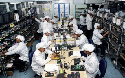
Om Nanotech Pvt. Ltd. the leading manufacturer, supplier and exporter of Memory Modules, Computer RAM, Pen Drives, Flash Cards, has been leading in innovation and bringing first-time technologies to India. After successfully establishing DRAM/Flash IC calibration/testing, Om Nanotech Pvt. Ltd. has now ventured into Die Testing for DRAM/Flash, which is again a First in India.
Om Nanotech- Shining Star in the Indian IT Industry
New Delhi, India | Posted on August 2nd, 2011Explaining the die testing facility at Om Nanotech�s manufacturing unit, Mr. Atul Khosla, Director, Om Nanotech Pvt. Ltd. said, "The Die Testing is a complex process which testing the Die before it is converted to an IC. Die is made from Wafers that are manufactured in highly complex FABS. There are only a handful of DRAM/FLASH FABs globally. Wafers are very thin disks of pure silicon on which minute circuits are etched using very nano-meter lasers. The wafer could have hundreds of Dies� (circuits) etched in a single wafer. These wafers normally come in 8", 10" and 12" diameter sizes, which are then cut to produce Die. Die can be perceived as the smallest unit which independently has the complete functionality desired from the IC. This Die is subsequently sent for packaging which involves encapsulating the Die with special plastics (black colored body), after connecting the connector pads on the Die to external terminals using extremely thin gold wires. Die probing requires specialized probes that need handling under a microscope."
"Along with its contribution in the manufacturing of memory products, we are proud that our manufacturing unit has also resulted as a source of employment for a number of people," added Mr. Khosla.
At the die testing facility, Om Nanotech conducts die probing which ensures that the Die has no inherent problems that may result in low yields after the Die has been packaged into IC . Obviously, the Die that is faulty, results in a faulty packaged IC, leading to wastage of investment on the packaging itself
To master this technology, Om Nanotech Pvt. Ltd. Organized specialized overseas training. The team got extended training and successfully replicated Die Testing at it�s Noida facility, without any further assistance from any external party. Om Nanotech Pvt. Ltd. has currently established a Die Testing capacity of 9 million die per annum.
####
About Om Nanotech Pvt. Ltd.
OM Nanotech Pvt. Ltd. is the largest exporter of memory modules and Flash products, operating from a 24,000 sq. ft. ISO 9000:2008, a state-of-art facility out of NSEZ, Noida. Om Nanotech is probably the First facility in India to undertake DRAM and Flash IC testing and Die testing, With a well-trained manpower of 450 working out of largest-of-its-kind facility in India, Om Nanotech has following production capacities:
Memory Modules: 2.5 million per year
Dram IC Testing: 40 million per year
Flash IC Testing: 9 million per year
Flash Drive : 0.6 million per year
Die Testing: 9 million per year
The manufacturer, Om Nanotech Pvt Ltd., subsidiary of Om Associates Pte Ltd, Singapore, is the recipient of �Best Exporter� award for 2007-08 and 2008 - 09 from Ministry of Commerce. The parent company has also bagged many awards in Singapore like Part of Top 50 Fastest Growing Companies in Singapore - Enterprise 50 (2010), Top Entrepreneur of the Year 2010, Entrepreneur of the Year 2010 (SICCI), Global Trader Award 2009 etc.
For more information, please click here
Contacts:
Alliance Public Relations Pvt. Ltd.
D-1/14,Hauz Khas,
New Delhi-110 016
Tel:
E-Mail:-
www.proalliancepr.com
Copyright © Om Nanotech Pvt. Ltd.
If you have a comment, please Contact us.Issuers of news releases, not 7th Wave, Inc. or Nanotechnology Now, are solely responsible for the accuracy of the content.
Bookmark:


| Related News Press |
News and information
![]() Simulating magnetization in a Heisenberg quantum spin chain April 5th, 2024
Simulating magnetization in a Heisenberg quantum spin chain April 5th, 2024
![]() NRL charters Navy�s quantum inertial navigation path to reduce drift April 5th, 2024
NRL charters Navy�s quantum inertial navigation path to reduce drift April 5th, 2024
![]() Discovery points path to flash-like memory for storing qubits: Rice find could hasten development of nonvolatile quantum memory April 5th, 2024
Discovery points path to flash-like memory for storing qubits: Rice find could hasten development of nonvolatile quantum memory April 5th, 2024
Chip Technology
![]() Discovery points path to flash-like memory for storing qubits: Rice find could hasten development of nonvolatile quantum memory April 5th, 2024
Discovery points path to flash-like memory for storing qubits: Rice find could hasten development of nonvolatile quantum memory April 5th, 2024
![]() Utilizing palladium for addressing contact issues of buried oxide thin film transistors April 5th, 2024
Utilizing palladium for addressing contact issues of buried oxide thin film transistors April 5th, 2024
![]() HKUST researchers develop new integration technique for efficient coupling of III-V and silicon February 16th, 2024
HKUST researchers develop new integration technique for efficient coupling of III-V and silicon February 16th, 2024
Memory Technology
![]() Utilizing palladium for addressing contact issues of buried oxide thin film transistors April 5th, 2024
Utilizing palladium for addressing contact issues of buried oxide thin film transistors April 5th, 2024
![]() Interdisciplinary: Rice team tackles the future of semiconductors Multiferroics could be the key to ultralow-energy computing October 6th, 2023
Interdisciplinary: Rice team tackles the future of semiconductors Multiferroics could be the key to ultralow-energy computing October 6th, 2023
![]() Researchers discover materials exhibiting huge magnetoresistance June 9th, 2023
Researchers discover materials exhibiting huge magnetoresistance June 9th, 2023
Announcements
![]() NRL charters Navy�s quantum inertial navigation path to reduce drift April 5th, 2024
NRL charters Navy�s quantum inertial navigation path to reduce drift April 5th, 2024
![]() Discovery points path to flash-like memory for storing qubits: Rice find could hasten development of nonvolatile quantum memory April 5th, 2024
Discovery points path to flash-like memory for storing qubits: Rice find could hasten development of nonvolatile quantum memory April 5th, 2024
Photonics/Optics/Lasers
![]() With VECSELs towards the quantum internet Fraunhofer: IAF achieves record output power with VECSEL for quantum frequency converters April 5th, 2024
With VECSELs towards the quantum internet Fraunhofer: IAF achieves record output power with VECSEL for quantum frequency converters April 5th, 2024
![]() Nanoscale CL thermometry with lanthanide-doped heavy-metal oxide in TEM March 8th, 2024
Nanoscale CL thermometry with lanthanide-doped heavy-metal oxide in TEM March 8th, 2024
![]() Optically trapped quantum droplets of light can bind together to form macroscopic complexes March 8th, 2024
Optically trapped quantum droplets of light can bind together to form macroscopic complexes March 8th, 2024
![]() HKUST researchers develop new integration technique for efficient coupling of III-V and silicon February 16th, 2024
HKUST researchers develop new integration technique for efficient coupling of III-V and silicon February 16th, 2024
|
|
||
|
|
||
| The latest news from around the world, FREE | ||
|
|
||
|
|
||
| Premium Products | ||
|
|
||
|
Only the news you want to read!
Learn More |
||
|
|
||
|
Full-service, expert consulting
Learn More |
||
|
|
||