Home > Press > Foreign-Born Scientists Contribute to U.S. Nanotechnology Innovation
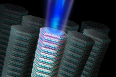 |
| One example of nanotechnology is this nanowire laser, a device in development in the laboratory of 2007 National Science Foundation Waterman awardee Peidong Yang of the University of California, Berkeley. Credit: Nicolle Rager Fuller/NSF |
Abstract:
Researchers at the Center for Nanotechnology in Society at the University of California, Santa Barbara (CNS-UCSB), a center supported by NSF (award number 0938099), examined the contributions of foreign-born scientists to nanotechnology innovation. They looked at authorship of the top one percent of the most highly-cited articles on nanotechnology by U.S. scientists and engineers between 1999-2009.
Foreign-Born Scientists Contribute to U.S. Nanotechnology Innovation
Arlington, VA | Posted on July 5th, 2011While the role of foreign-born scientists in information technology and biotechnology innovation has been well studied, comparable studies on nanotechnology have been conspicuously absent. The prevalence of the foreign born in the American general population and scientific labor force was used as the benchmark for expected contributions to the nanotechnology industry. Research results concluded that the prevalence of foreign-born authors in nanotechnology publications exceeded that of the general population and the U.S. scientific community. Besides the U.S. (47 scientists), significant contributions came from China (21 scientists), India (eight scientists), and Germany (five scientists), and foreign-born contributions have steadily increased from 38 percent in 1999 to 73 percent in 2009. These findings point to the significance of non-native researchers in promoting U.S. nanotechnology innovation and indicate significant globalization within the American scientific and engineering communities.
####
For more information, please click here
Copyright © National Science Foundation
If you have a comment, please Contact us.Issuers of news releases, not 7th Wave, Inc. or Nanotechnology Now, are solely responsible for the accuracy of the content.
Bookmark:


| Related News Press |
News and information
![]() Decoding hydrogen‑bond network of electrolyte for cryogenic durable aqueous zinc‑ion batteries January 30th, 2026
Decoding hydrogen‑bond network of electrolyte for cryogenic durable aqueous zinc‑ion batteries January 30th, 2026
![]() COF scaffold membrane with gate‑lane nanostructure for efficient Li+/Mg2+ separation January 30th, 2026
COF scaffold membrane with gate‑lane nanostructure for efficient Li+/Mg2+ separation January 30th, 2026
Govt.-Legislation/Regulation/Funding/Policy
![]() Metasurfaces smooth light to boost magnetic sensing precision January 30th, 2026
Metasurfaces smooth light to boost magnetic sensing precision January 30th, 2026
![]() New imaging approach transforms study of bacterial biofilms August 8th, 2025
New imaging approach transforms study of bacterial biofilms August 8th, 2025
![]() Electrifying results shed light on graphene foam as a potential material for lab grown cartilage June 6th, 2025
Electrifying results shed light on graphene foam as a potential material for lab grown cartilage June 6th, 2025
Announcements
![]() Decoding hydrogen‑bond network of electrolyte for cryogenic durable aqueous zinc‑ion batteries January 30th, 2026
Decoding hydrogen‑bond network of electrolyte for cryogenic durable aqueous zinc‑ion batteries January 30th, 2026
![]() COF scaffold membrane with gate‑lane nanostructure for efficient Li+/Mg2+ separation January 30th, 2026
COF scaffold membrane with gate‑lane nanostructure for efficient Li+/Mg2+ separation January 30th, 2026
Interviews/Book Reviews/Essays/Reports/Podcasts/Journals/White papers/Posters
![]() Metasurfaces smooth light to boost magnetic sensing precision January 30th, 2026
Metasurfaces smooth light to boost magnetic sensing precision January 30th, 2026
![]() COF scaffold membrane with gate‑lane nanostructure for efficient Li+/Mg2+ separation January 30th, 2026
COF scaffold membrane with gate‑lane nanostructure for efficient Li+/Mg2+ separation January 30th, 2026
|
|
||
|
|
||
| The latest news from around the world, FREE | ||
|
|
||
|
|
||
| Premium Products | ||
|
|
||
|
Only the news you want to read!
Learn More |
||
|
|
||
|
Full-service, expert consulting
Learn More |
||
|
|
||