Home > Press > Imaging of surface plasmons may be a lot easier than you thought
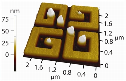 |
| Surface plasmon patterns can be imprinted on metallic nanostructures for subsequent high resolution imaging with standard surface probe techniques. |
Abstract:
An unusual observation turned into a scientific breakthrough when K.U.Leuven researchers investigating the optical properties of nanomaterials discovered that so-called surface plasmons leave imprints on the surface of the nanostructures. This leads to a new type of high resolution microscopy for imaging the electric fields of nanostructures.
Imaging of surface plasmons may be a lot easier than you thought
Leuven, Belgium | Posted on June 8th, 2011Nanomaterials, consisting of extremely small particles or thin layers, tend to acquire unexpected properties. Optical nanomaterials are a class of materials that have emerged over the last ten years and that have quickly become a hot topic in material science due to their counterintuitive optical behavior and revolutionary potential applications. Optical nanomaterials are mainly based on surface plasmon resonances - the property whereby, in metallic nanostructures, light can collectively excite surface electron waves. These electron waves have the same frequency as light, but much shorter wavelengths, which allow their manipulation at the nanoscale. In other words, with the help of plasmons, light can be captured, modified and even stored in nanostructures. This emerging technology finds applications in surprising areas, ranging from cancer treatment (by targeting cancer cells with nanoparticles that will produce heat when excited) to invisibility (by causing light to follow a trail of nanoparticles, that acts as an invisibility cloak to whatever is underneath them).
The imaging of surface plasmons provides a direct way to map and understand the local electric fields that are responsible for the unusual electromagnetic properties of optical nanomaterials. However, the imaging of surface plasmons is quite challenging. While there are methods to image plasmons with high resolution, they come at a considerable increase in both cost and complexity. But now, Ventsislav K. Valev and his colleagues have demonstrated a powerful and user friendly method for imaging plasmonic patterns in nanostructures.
"We were performing routine characterization of freshly grown samples, when I asked Yogesh, one of our Ph.D. students, to look at a sample that had already been studied. There was absolutely no reason to do this; I just had a hunch," sais Ventsislav Valev. "Surprisingly, this sample appeared to be decorated and I immediately recognized the pattern. Somehow, the optical properties have been imprinted on the surface of the nanostructures."
The scientists indeed found out that upon illuminating nanostructures made of nickel or palladium, the resulting surface plasmon pattern is imprinted on the structures themselves. This imprinting is done through displacing material from the nanostructure to the regions where the plasmon enhancements are the largest. In this manner, the plasmons are effectively decorated, allowing for subsequent imaging with standard surface probe techniques, such as scanning electron microscopy or atomic force microscopy. The imprinting method is quite unique, combining aspects of both imaging and writing techniques.
This research is described in an upcoming paper in the journal Physical Review Letters.
Full bibliographic information
V. K. Valev, A. V. Silhanek, Y. Jeyaram, D. Denkova, B. De Clercq, V. Petkov, X. Zheng, V. Volskiy, W. Gillijns, G. A. E. Vandenbosch, O. A. Aktsipetrov, M. Ameloot, V. V. Moshchalkov and T. Verbiest, "Hotspot Decorations Map Plasmonic Patterns with the Resolution of Scanning Probe Techniques", Phys. Rev. Lett. 106, 226803 (2011), prl.aps.org/abstract/PRL/v106/i22/e226803.
####
For more information, please click here
Contacts:
Griet Van der Perre
+32 16 32 40 08
Copyright © AlphaGalileo
If you have a comment, please Contact us.Issuers of news releases, not 7th Wave, Inc. or Nanotechnology Now, are solely responsible for the accuracy of the content.
Bookmark:


| Related Links |
| Related News Press |
News and information
![]() Quantum computer improves AI predictions April 17th, 2026
Quantum computer improves AI predictions April 17th, 2026
![]() Flexible sensor gains sensitivity under pressure April 17th, 2026
Flexible sensor gains sensitivity under pressure April 17th, 2026
![]() A reusable chip for particulate matter sensing April 17th, 2026
A reusable chip for particulate matter sensing April 17th, 2026
![]() Detecting vibrational quantum beating in the predissociation dynamics of SF6 using time-resolved photoelectron spectroscopy April 17th, 2026
Detecting vibrational quantum beating in the predissociation dynamics of SF6 using time-resolved photoelectron spectroscopy April 17th, 2026
Imaging
![]() Simple algorithm paired with standard imaging tool could predict failure in lithium metal batteries August 8th, 2025
Simple algorithm paired with standard imaging tool could predict failure in lithium metal batteries August 8th, 2025
Discoveries
![]() Quantum computer improves AI predictions April 17th, 2026
Quantum computer improves AI predictions April 17th, 2026
![]() Flexible sensor gains sensitivity under pressure April 17th, 2026
Flexible sensor gains sensitivity under pressure April 17th, 2026
![]() A reusable chip for particulate matter sensing April 17th, 2026
A reusable chip for particulate matter sensing April 17th, 2026
![]() Detecting vibrational quantum beating in the predissociation dynamics of SF6 using time-resolved photoelectron spectroscopy April 17th, 2026
Detecting vibrational quantum beating in the predissociation dynamics of SF6 using time-resolved photoelectron spectroscopy April 17th, 2026
Announcements
![]() A fundamentally new therapeutic approach to cystic fibrosis: Nanobody repairs cellular defect April 17th, 2026
A fundamentally new therapeutic approach to cystic fibrosis: Nanobody repairs cellular defect April 17th, 2026
![]() UC Irvine physicists discover method to reverse �quantum scrambling� : The work addresses the problem of information loss in quantum computing system April 17th, 2026
UC Irvine physicists discover method to reverse �quantum scrambling� : The work addresses the problem of information loss in quantum computing system April 17th, 2026
Tools
![]() Metasurfaces smooth light to boost magnetic sensing precision January 30th, 2026
Metasurfaces smooth light to boost magnetic sensing precision January 30th, 2026
![]() From sensors to smart systems: the rise of AI-driven photonic noses January 30th, 2026
From sensors to smart systems: the rise of AI-driven photonic noses January 30th, 2026
![]() Japan launches fully domestically produced quantum computer: Expo visitors to experience quantum computing firsthand August 8th, 2025
Japan launches fully domestically produced quantum computer: Expo visitors to experience quantum computing firsthand August 8th, 2025
|
|
||
|
|
||
| The latest news from around the world, FREE | ||
|
|
||
|
|
||
| Premium Products | ||
|
|
||
|
Only the news you want to read!
Learn More |
||
|
|
||
|
Full-service, expert consulting
Learn More |
||
|
|
||