Home > Press > New electronics material closer to commercial reality
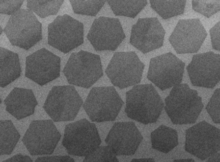 |
| This scanning electron microscope picture shows individual crystal "grains" in an array of a material called graphene. Researchers have developed a method for creating the arrays, an advancement that opens up the possibility of a replacement for silicon in high-performance computers and electronics. (Image Care of University of Houston) |
Abstract:
Control and Characterization of Individual Grains and Grain Boundaries in Graphene Grown by Chemical Vapour Deposition
Qingkai Yu1,2*, Luis A. Jauregui3,WeiWu1, Robert Colby4, Jifa Tian5, Zhihua Su6, Helin Cao5, Zhihong Liu6, Deepak Pandey5, DongguangWei7, Ting Fung Chung5, Peng Peng1, Nathan Guisinger8, Eric A. Stach 4,9, Jiming Bao6 , Shin-Shem Pei1 and Yong P. Chen 10*
The strong interest in graphene has motivated the scalable production of high quality graphene and graphene devices. As the large-scale graphene films synthesized to date are typically polycrystalline, it is important to characterize and control grain boundaries, generally believed to degrade graphene quality. Here we study single-crystal graphene grains synthesized by ambient CVD on polycrystalline Cu, and show how individual boundaries between coalescing grains affect graphene's electronic properties. The graphene grains show no definite epitaxial relationship with the Cu substrate, and can cross Cu grain boundaries. The edges of these grains are found to be predominantly parallel to zigzag directions. We show that grain boundaries give a significant Raman ‘D' peak, impede electrical transport, and induce prominent weak localization indicative of intervalley scattering in graphene . Finally, we demonstrate an approach using pre-patterned growth seeds to control graphene nucleation, opening a route toward scalable fabrication of single-crystal graphene devices without grain boundaries.
New electronics material closer to commercial reality
West Lafayette, IN | Posted on May 25th, 2011Researchers have developed a method for creating single-crystal arrays of a material called graphene, an advance that opens up the possibility of a replacement for silicon in high-performance computers and electronics.
Graphene is a one-atom-thick layer of carbon that conducts electricity with little resistance or heat generation. The arrays could make possible a new class of high-speed transistors and integrated circuits that consume less energy than conventional silicon electronics.
The new findings represent an advance toward perfecting a method for manufacturing large quantities of single crystals of the material, similar to the production of silicon wafers.
"Graphene isn't there yet, in terms of high quality mass production like silicon, but this is a very important step in that direction," said Yong P. Chen, corresponding author for the new study and Miller Family Assistant Professor of Nanoscience and Physics at Purdue University.
Other researchers have grown single crystals of graphene, but no others have demonstrated how to create ordered arrays, or patterns that could be used to fabricate commercial electronic devices and integrated circuits.
The hexagonal single crystals are initiated from graphite "seeds" and then grown on top of a copper foil inside a chamber containing methane gas using a process called chemical vapor deposition. The seeded growth method, critical to the new findings, was invented by Qingkai Yu, co-corresponding author for the study and an assistant professor at Texas State University's Ingram School of Engineering.
"Using these seeds, we can grow an ordered array of thousands or millions of single crystals of graphene," said Yu, who pioneered the method while a researcher at the University of Houston. "We hope that industry will look at these findings and consider the ordered arrays as a possible means of fabricating electronic devices."
Findings are detailed in a research paper appearing online this week and in the June issue of Nature Materials. The work was conducted by researchers at Purdue, the University of Houston, Texas State University, Brookhaven National Laboratory, Argonne National Laboratories and Carl Zeiss SMT Inc.
Graphene currently is created in "polycrystalline" sheets made up of randomly positioned and irregularly shaped "grains" merged together. Having an ordered array means the positions of each crystal are predictable, and not random as they are in polycrystalline film.
The arrays enable researchers to precisely position electronic devices in each grain, which is a single crystal having a seamless lattice structure that improves electrical properties, said Eric Stach, a researcher at Brookhaven and former Purdue professor of materials engineering.
The new research findings confirmed a theory that the flow of electrons is hindered at the point where one grain meets another. The arrays of single-crystal grains could eliminate that problem.
The researchers demonstrated that they could control the growth of the ordered arrays; were the first to demonstrate the electronic properties of individual grain boundaries; and they found that the edges of a single hexagonal crystal grain are parallel to well-defined directions in graphene's atomic lattice, revealing the orientation of each crystal.
Knowing the orientation is necessary to measure the precise properties of the crystals, providing information needed to create better electronic devices. To determine the orientation of the graphene lattice, the researchers used two kinds of advanced microscopy techniques known as transmission electron microscopy and scanning tunneling microscopy. The techniques provided extremely high-resolution images of individual carbon atoms making up graphene.
The electronic properties across the grain boundaries were measured using tiny electrodes connected to two adjoining grains.
Findings demonstrated a higher electrical resistance at the grain boundaries and also showed that the boundaries hinder electrical conduction due to scattering of electrons. That finding was correlated using another technique called Raman spectroscopy.
The paper was authored by Yu and Purdue graduate student Luis A. Jauregui, Houston graduate student Wei Wu, Purdue graduate student Robert Colby, Purdue postdoctoral researcher Jifa Tian, along with 12 other researchers including Stach and Chen.
Yu, Wu, Houston graduate student Zhihua Su and colleagues created graphene single crystals, including the ordered arrays for the research at the University of Houston. Chen, Jauregui, Tian and colleagues studied these hexagonal graphene crystals, their edges and the grain boundaries using Raman spectroscopy, scanning tunneling microscopy and electrical measurements. They have used various facilities in their Quantum Matter and Device Laboratory, Purdue's Birck Nanotechnology Center, as well as those in the National High Magnetic Field Laboratory and the Center for Nanoscale Materials at the Argonne National Laboratory. Stach and Colby documented the crystal orientation using transmission electron microscopes at Purdue's Birck Nanotechnology Center and at the Center for Functional Nanomaterials at the Brookhaven National Laboratory.
The research was supported through a variety of funding sources, including the National Science Foundation, the U.S. Department of Energy, the Department of Homeland Security, Defense Threat Reduction Agency, IBM Inc., the Welch Foundation, the Miller Family Endowment and Midwest Institute for Nanoelectronics Discovery.
####
For more information, please click here
Contacts:
Writer:
Emil Venere
765-494-4709
Sources:
Yong P. Chen
765- 494-0947
Qingkai Yu
(512) 245-4093
Eric Stach
(631) 344-2618
Rachel Twinn
Nature media contact in the United Kingdom
44-20-7843-4658
Neda Afsarmanesh
Nature North America media contact
212-726-9231
Copyright © Purdue University
If you have a comment, please Contact us.Issuers of news releases, not 7th Wave, Inc. or Nanotechnology Now, are solely responsible for the accuracy of the content.
Bookmark:


| Related Links |
![]() Download News and Views article in Nature
Download News and Views article in Nature
| Related News Press |
News and information
![]() Simulating magnetization in a Heisenberg quantum spin chain April 5th, 2024
Simulating magnetization in a Heisenberg quantum spin chain April 5th, 2024
![]() NRL charters Navy’s quantum inertial navigation path to reduce drift April 5th, 2024
NRL charters Navy’s quantum inertial navigation path to reduce drift April 5th, 2024
![]() Discovery points path to flash-like memory for storing qubits: Rice find could hasten development of nonvolatile quantum memory April 5th, 2024
Discovery points path to flash-like memory for storing qubits: Rice find could hasten development of nonvolatile quantum memory April 5th, 2024
Graphene/ Graphite
![]() NRL discovers two-dimensional waveguides February 16th, 2024
NRL discovers two-dimensional waveguides February 16th, 2024
Govt.-Legislation/Regulation/Funding/Policy
![]() NRL charters Navy’s quantum inertial navigation path to reduce drift April 5th, 2024
NRL charters Navy’s quantum inertial navigation path to reduce drift April 5th, 2024
![]() Discovery points path to flash-like memory for storing qubits: Rice find could hasten development of nonvolatile quantum memory April 5th, 2024
Discovery points path to flash-like memory for storing qubits: Rice find could hasten development of nonvolatile quantum memory April 5th, 2024
![]() Chemical reactions can scramble quantum information as well as black holes April 5th, 2024
Chemical reactions can scramble quantum information as well as black holes April 5th, 2024
Discoveries
![]() Chemical reactions can scramble quantum information as well as black holes April 5th, 2024
Chemical reactions can scramble quantum information as well as black holes April 5th, 2024
![]() New micromaterial releases nanoparticles that selectively destroy cancer cells April 5th, 2024
New micromaterial releases nanoparticles that selectively destroy cancer cells April 5th, 2024
![]() Utilizing palladium for addressing contact issues of buried oxide thin film transistors April 5th, 2024
Utilizing palladium for addressing contact issues of buried oxide thin film transistors April 5th, 2024
Announcements
![]() NRL charters Navy’s quantum inertial navigation path to reduce drift April 5th, 2024
NRL charters Navy’s quantum inertial navigation path to reduce drift April 5th, 2024
![]() Discovery points path to flash-like memory for storing qubits: Rice find could hasten development of nonvolatile quantum memory April 5th, 2024
Discovery points path to flash-like memory for storing qubits: Rice find could hasten development of nonvolatile quantum memory April 5th, 2024
Grants/Sponsored Research/Awards/Scholarships/Gifts/Contests/Honors/Records
![]() Discovery points path to flash-like memory for storing qubits: Rice find could hasten development of nonvolatile quantum memory April 5th, 2024
Discovery points path to flash-like memory for storing qubits: Rice find could hasten development of nonvolatile quantum memory April 5th, 2024
![]() Chemical reactions can scramble quantum information as well as black holes April 5th, 2024
Chemical reactions can scramble quantum information as well as black holes April 5th, 2024
|
|
||
|
|
||
| The latest news from around the world, FREE | ||
|
|
||
|
|
||
| Premium Products | ||
|
|
||
|
Only the news you want to read!
Learn More |
||
|
|
||
|
Full-service, expert consulting
Learn More |
||
|
|
||