Home > Press > NIST, AIP to Make Semiconductor Research Freely Available Online
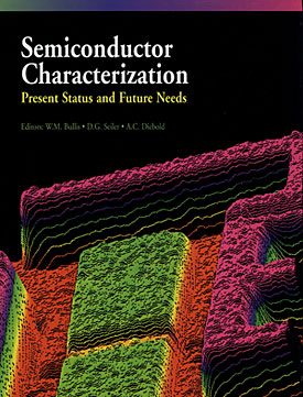 |
| Proceedings that have been available through paid subscription or compendium volumes, such as this one from the conference's first year, are now available online at no charge. Credit: AIP |
Abstract:
A wealth of information on recent advances in semiconductor research is now available for free, thanks to an agreement between the National Institute of Standards and Technology (NIST) and the American Institute of Physics (AIP). The development should be welcome news to semiconductor chip manufacturers, universities and others in the computer industry who will find it less expensive to explore changes in critical measurements for semiconductor technology.
NIST, AIP to Make Semiconductor Research Freely Available Online
Gaithersburg, MD | Posted on May 25th, 2011The two institutions have made the proceedings from the International Conference on Frontiers of Characterization and Metrology for Nanoelectronics (formerly Characterization and Metrology for ULSI Technology) available for free download from both their Web sites. Until now, papers presented at the NIST-led conference series, which began in 1995, were only available through paid subscriptions.
NIST's David Seiler says the proceedings' availability should greatly help employees in the fast-paced semiconductor industry get up to speed on unfamiliar measurement and characterization issues. In addition, they can learn about new techniques and equipment being introduced to characterize semiconductors.
"These collected proceedings represent research and overviews of critical topics collected from worldwide experts in the field of semiconductor characterization and metrology," says Seiler. "As there is frequent turnover in the industry, there is constant need for training and retraining of employees. Improved access to this background will ease that process dramatically."
On the NIST Web site, the archived proceedings publications, up to and including the 2009 conference (along with slides from most of the conference invited talks), are available at www.nist.gov/pml/semiconductor/conference/archives.cfm. The AIP has made the archived proceedings publications available at proceedings.aip.org/semiconductor_metrology. Documents are available in searchable PDF form.
The eighth conference in the series is being held this week (May 23-26, 2011) at the MINATEC Campus in Grenoble, France. Proceedings from this week's conference will be available online in the near future. Information about AIP is available at www.aip.org/aip.
####
About NIST
The National Institute of Standards and Technology (NIST) is an agency of the U.S. Department of Commerce.
For more information, please click here
Contacts:
Chad Boutin
(301) 975-4261
Copyright © NIST
If you have a comment, please Contact us.Issuers of news releases, not 7th Wave, Inc. or Nanotechnology Now, are solely responsible for the accuracy of the content.
Bookmark:


| Related News Press |
News and information
![]() Simulating magnetization in a Heisenberg quantum spin chain April 5th, 2024
Simulating magnetization in a Heisenberg quantum spin chain April 5th, 2024
![]() NRL charters Navy�s quantum inertial navigation path to reduce drift April 5th, 2024
NRL charters Navy�s quantum inertial navigation path to reduce drift April 5th, 2024
![]() Discovery points path to flash-like memory for storing qubits: Rice find could hasten development of nonvolatile quantum memory April 5th, 2024
Discovery points path to flash-like memory for storing qubits: Rice find could hasten development of nonvolatile quantum memory April 5th, 2024
Laboratories
![]() A battery�s hopping ions remember where they�ve been: Seen in atomic detail, the seemingly smooth flow of ions through a battery�s electrolyte is surprisingly complicated February 16th, 2024
A battery�s hopping ions remember where they�ve been: Seen in atomic detail, the seemingly smooth flow of ions through a battery�s electrolyte is surprisingly complicated February 16th, 2024
![]() NRL discovers two-dimensional waveguides February 16th, 2024
NRL discovers two-dimensional waveguides February 16th, 2024
![]() Three-pronged approach discerns qualities of quantum spin liquids November 17th, 2023
Three-pronged approach discerns qualities of quantum spin liquids November 17th, 2023
Chip Technology
![]() Discovery points path to flash-like memory for storing qubits: Rice find could hasten development of nonvolatile quantum memory April 5th, 2024
Discovery points path to flash-like memory for storing qubits: Rice find could hasten development of nonvolatile quantum memory April 5th, 2024
![]() Utilizing palladium for addressing contact issues of buried oxide thin film transistors April 5th, 2024
Utilizing palladium for addressing contact issues of buried oxide thin film transistors April 5th, 2024
![]() HKUST researchers develop new integration technique for efficient coupling of III-V and silicon February 16th, 2024
HKUST researchers develop new integration technique for efficient coupling of III-V and silicon February 16th, 2024
Announcements
![]() NRL charters Navy�s quantum inertial navigation path to reduce drift April 5th, 2024
NRL charters Navy�s quantum inertial navigation path to reduce drift April 5th, 2024
![]() Discovery points path to flash-like memory for storing qubits: Rice find could hasten development of nonvolatile quantum memory April 5th, 2024
Discovery points path to flash-like memory for storing qubits: Rice find could hasten development of nonvolatile quantum memory April 5th, 2024
Events/Classes
![]() Researchers demonstrate co-propagation of quantum and classical signals: Study shows that quantum encryption can be implemented in existing fiber networks January 20th, 2023
Researchers demonstrate co-propagation of quantum and classical signals: Study shows that quantum encryption can be implemented in existing fiber networks January 20th, 2023
Alliances/Trade associations/Partnerships/Distributorships
![]() Chicago Quantum Exchange welcomes six new partners highlighting quantum technology solutions, from Chicago and beyond September 23rd, 2022
Chicago Quantum Exchange welcomes six new partners highlighting quantum technology solutions, from Chicago and beyond September 23rd, 2022
![]() University of Illinois Chicago joins Brookhaven Lab's Quantum Center June 10th, 2022
University of Illinois Chicago joins Brookhaven Lab's Quantum Center June 10th, 2022
|
|
||
|
|
||
| The latest news from around the world, FREE | ||
|
|
||
|
|
||
| Premium Products | ||
|
|
||
|
Only the news you want to read!
Learn More |
||
|
|
||
|
Full-service, expert consulting
Learn More |
||
|
|
||