Home > Press > Empa opens laser centre in Thun - Large surfaces can be machined with nanometre precision
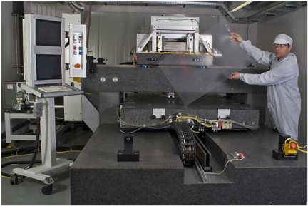 |
| Karl B�hlen, director of Crealas GmbH, at work in the new laser centre. |
Abstract:
On 7 April 2011, in the presence of its Director, Gian-Luca Bona, and the Mayor of Thun, Raphael Lanz, Empa's new laser centre, which houses the only UV laser facility of its kind in the world, was opened in Thun. The facility will help researchers to develop new kinds of surfaces. Commercial partners will be able to use it to structure large films with micro to nanometre precision.
Empa opens laser centre in Thun - Large surfaces can be machined with nanometre precision
Thun, Switzerland | Posted on April 9th, 2011Now very large surfaces can be microstructured at Empa's new laser centre in Thun. Centrepiece of the facility, which is run by Empa in close collaboration with Crealas GmbH - one of only three worldwide - is a pulsed ultraviolet (UV) laser beam, which ablates nanometre-thin layers precisely from large surfaces of up to three square metres. A granite table weighing 19 tonnes acts as the base and this was transported to Thun in dramatic fashion in October 2010.
Materials with new physico-mechanical properties
Surface microstructuring creates new physico-mechanical properties. For example, the microstructures can reduce friction, lower the amount of drag or inhibit fungal growth. Films for optical structures with light-controlling properties can also be manufactured, for example 3D screens that work without glasses. Patrik Hoffman, Head of Empa's "Advanced Materials Processing" laboratory, imagines using it to develop new kinds of windowpanes which would light up internal spaces at night and act as solar cells during the day. He also has the intention of creating materials for electrochemical processes, using them to form electrical connections on flexible screens or solar cells.
Unique services to industry
Not only will materials science benefit from the new facility, it also offers new prospects to Empa's commercial partners. The laser machining of large surface areas means moulding tools can be manufactured. Industry needs these in order to produce structured films cheaply and in bulk. Until now, moulding tools have always had to be assembled from several parts, whereas the new laser centre enables them to be produced in a single piece.
Films for optical security features can also be manufactured at the facility. A number of countries are already trying to replace the holograms on their banknotes with microstructured films with optical 3D effects. Empa Director Gian-Luca Bona said: "The new laser centre means we can offer services that are unique in Switzerland. This will open up completely new opportunities for both our commercial and research partners."
####
For more information, please click here
Contacts:
Prof. Dr. Patrik Hoffmann
Empa
Advanced Materials Processing
Tel. +41 33 228 29 45
Dr. Karl Boehlen
Empa
Advanced Materials Processing/Managing Director Crealas GmbH
Tel. +41 33 228 40 21
Editor / Media contact
Martina Peter
Empa
Communications
Tel. +41 58 765 49 87
Copyright © AlphaGalileo
If you have a comment, please Contact us.Issuers of news releases, not 7th Wave, Inc. or Nanotechnology Now, are solely responsible for the accuracy of the content.
Bookmark:


| Related News Press |
News and information
![]() Simulating magnetization in a Heisenberg quantum spin chain April 5th, 2024
Simulating magnetization in a Heisenberg quantum spin chain April 5th, 2024
![]() NRL charters Navy�s quantum inertial navigation path to reduce drift April 5th, 2024
NRL charters Navy�s quantum inertial navigation path to reduce drift April 5th, 2024
![]() Discovery points path to flash-like memory for storing qubits: Rice find could hasten development of nonvolatile quantum memory April 5th, 2024
Discovery points path to flash-like memory for storing qubits: Rice find could hasten development of nonvolatile quantum memory April 5th, 2024
![]() Good as gold - improving infectious disease testing with gold nanoparticles April 5th, 2024
Good as gold - improving infectious disease testing with gold nanoparticles April 5th, 2024
Thin films
![]() Utilizing palladium for addressing contact issues of buried oxide thin film transistors April 5th, 2024
Utilizing palladium for addressing contact issues of buried oxide thin film transistors April 5th, 2024
![]() Understanding the mechanism of non-uniform formation of diamond film on tools: Paving the way to a dry process with less environmental impact March 24th, 2023
Understanding the mechanism of non-uniform formation of diamond film on tools: Paving the way to a dry process with less environmental impact March 24th, 2023
![]() New study introduces the best graphite films: The work by Distinguished Professor Feng Ding at UNIST has been published in the October 2022 issue of Nature Nanotechnology November 4th, 2022
New study introduces the best graphite films: The work by Distinguished Professor Feng Ding at UNIST has been published in the October 2022 issue of Nature Nanotechnology November 4th, 2022
![]() Thin-film, high-frequency antenna array offers new flexibility for wireless communications November 5th, 2021
Thin-film, high-frequency antenna array offers new flexibility for wireless communications November 5th, 2021
![]() Leibniz Prize winner Professor Dr. Oliver G. Schmidt moves to Chemnitz University of Technology: President Professor Dr. Gerd Strohmeier refers to an 'absolute top transfer' September 10th, 2021
Leibniz Prize winner Professor Dr. Oliver G. Schmidt moves to Chemnitz University of Technology: President Professor Dr. Gerd Strohmeier refers to an 'absolute top transfer' September 10th, 2021
Openings/New facilities/Groundbreaking/Expansion
![]() OCSiAl expands its graphene nanotube production capacities to Europe June 17th, 2022
OCSiAl expands its graphene nanotube production capacities to Europe June 17th, 2022
![]() GLOBALFOUNDRIES Moves Corporate Headquarters to its Most Advanced Semiconductor Manufacturing Facility in New York April 27th, 2021
GLOBALFOUNDRIES Moves Corporate Headquarters to its Most Advanced Semiconductor Manufacturing Facility in New York April 27th, 2021
Announcements
![]() NRL charters Navy�s quantum inertial navigation path to reduce drift April 5th, 2024
NRL charters Navy�s quantum inertial navigation path to reduce drift April 5th, 2024
![]() Discovery points path to flash-like memory for storing qubits: Rice find could hasten development of nonvolatile quantum memory April 5th, 2024
Discovery points path to flash-like memory for storing qubits: Rice find could hasten development of nonvolatile quantum memory April 5th, 2024
Photonics/Optics/Lasers
![]() With VECSELs towards the quantum internet Fraunhofer: IAF achieves record output power with VECSEL for quantum frequency converters April 5th, 2024
With VECSELs towards the quantum internet Fraunhofer: IAF achieves record output power with VECSEL for quantum frequency converters April 5th, 2024
![]() Nanoscale CL thermometry with lanthanide-doped heavy-metal oxide in TEM March 8th, 2024
Nanoscale CL thermometry with lanthanide-doped heavy-metal oxide in TEM March 8th, 2024
![]() Optically trapped quantum droplets of light can bind together to form macroscopic complexes March 8th, 2024
Optically trapped quantum droplets of light can bind together to form macroscopic complexes March 8th, 2024
![]() HKUST researchers develop new integration technique for efficient coupling of III-V and silicon February 16th, 2024
HKUST researchers develop new integration technique for efficient coupling of III-V and silicon February 16th, 2024
Alliances/Trade associations/Partnerships/Distributorships
![]() Chicago Quantum Exchange welcomes six new partners highlighting quantum technology solutions, from Chicago and beyond September 23rd, 2022
Chicago Quantum Exchange welcomes six new partners highlighting quantum technology solutions, from Chicago and beyond September 23rd, 2022
![]() University of Illinois Chicago joins Brookhaven Lab's Quantum Center June 10th, 2022
University of Illinois Chicago joins Brookhaven Lab's Quantum Center June 10th, 2022
|
|
||
|
|
||
| The latest news from around the world, FREE | ||
|
|
||
|
|
||
| Premium Products | ||
|
|
||
|
Only the news you want to read!
Learn More |
||
|
|
||
|
Full-service, expert consulting
Learn More |
||
|
|
||