Home > Press > Zinc stannate nanostructures: growing a highly useful semiconductor
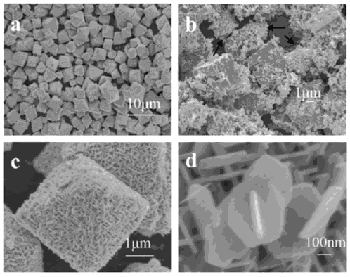 |
| Figure 1: Scanning electron microscope images of ZTO microstructures: (a) low magnification image of the Zn2SnO4 octahedrons; (b) ZnSn(OH)6 cubes formed in the initial stage of the reaction (note secondary nucleation on the cube surfaces); (c) a Zn2SnO4 octahedron; (d) coalescing nanoplates. (Reproduced with permission, � 2010 Elsevier B.V.) |
Abstract:
This timely review focuses on the synthesis of zinc stannate (zinc tin oxide: ZTO) nanostructures by the hydrothermal method, as well as the physical properties and applications of different zinc stannate nanostructures in solar cells, gas sensors, and photocatalysts.
Zinc stannate nanostructures: growing a highly useful semiconductor
Tsukuba, Japan | Posted on March 24th, 2011The review is published in March 2011 in the journal Science and Technology of Advanced MaterialsVol. 12(2011) p. 013004. Itis presented by Sunandan Baruah and Joydeep Dutta from the Asian Institute of Technology, Klong Luang, Thailand.
Binary semiconducting oxide nanostructures, such as zinc oxide and titanium oxide, are widely used in sensors and catalysts. However, ternary semiconducting oxide nanostructures, which show higher electrical conductivity and are more stable than the binary type, are increasingly in demand for specific applications due to their particular physical properties. In contrast to conventional �top-down' processes involving physically breaking large macroscopic materials into nanoparticles, the chemically based �self-organization' approach offers an inexpensive and flexible means of precisely controlling the size, crystal structure and optoelectronic properties of semiconducting oxide nanostructures, which is crucial for the use of ZTO in specific applications.
ZTO nanostructures can be produced using a variety of methods including thermal evaporation, high-temperature calcination, mechanical grinding, sol-gel synthesis, hydrothermal reaction, and ion-exchange reaction. Different methods produce different ratios of ZTO oxides and impurities, expressed in alternative crystal structures. The authors describe the pertinent features of the hydrothermal growth method for synthesizing ZTO, including high purity of the stable zinc orthostannate Zn2SnO4 and the accompanying �cubic spinel' crystal structure. Moreover, hydrothermal growth is an attractive and relatively simple method since crystal growth occurs at mild temperatures in water.
Typical hydrothermal growth of ZTO nanostructures consists of using an aqueous mixture of a zinc salt, such as zinc nitrate or zinc chloride, and stannic chloride. This mixture is then reduced at 200-250 �C in sodium hydroxide or ammonium hydroxide in a high-pressure environment. Various methods for hydrothermal growth of ZTO nanostructures are detailed by the authors, with varying end products in terms of crystal structure and �phase composition' - amounts of the particular oxides produced.
The physical properties of ZTO depend on the method used for their synthesis. ZTO is a �wide-gap' semiconductor with a bandgap of around 3.6 eV, but the precise bandgap energy depends on the conditions of synthesis, which might result in quantum confinement effects arising from the small size of the nanostructures. Controlling the photoelectrochemical properties of ZTO has practical importance, and relating the optical and electronic properties of ZTO with the composition and crystal structure can pave the way for applications of other complex oxides.
The authors describe industrial applications arising from the photoelectrochemical properties of ZTO. Firstly, as a photocatalyst ZTO can be used for degrading harmful pesticides from ground water; secondly the porous nanostructures are ideal for gas sensing as they offer high surface to volume ratios; and thirdly ZTO has potential in the field of dye-sensitized solar cells, an economically plausible alternative to conventional solar cells. Given that only a few morphologies have been reported, the authors conjecture that within the next decade ZTO nanostructures will find uses in further industrial applications.
This review contains 131 references and 22 figures and provides an invaluable source of up-to-date information for newcomers and experts in this exciting area of research.
####
Contacts:
National Institute for Materials Science
Tsukuba, Japan
Email:
Tel. +81-(0)29-859-2494
Copyright © National Institute for Materials Science
If you have a comment, please Contact us.Issuers of news releases, not 7th Wave, Inc. or Nanotechnology Now, are solely responsible for the accuracy of the content.
Bookmark:


| Related Links |
| Related News Press |
News and information
![]() Quantum computer improves AI predictions April 17th, 2026
Quantum computer improves AI predictions April 17th, 2026
![]() Flexible sensor gains sensitivity under pressure April 17th, 2026
Flexible sensor gains sensitivity under pressure April 17th, 2026
![]() A reusable chip for particulate matter sensing April 17th, 2026
A reusable chip for particulate matter sensing April 17th, 2026
![]() Detecting vibrational quantum beating in the predissociation dynamics of SF6 using time-resolved photoelectron spectroscopy April 17th, 2026
Detecting vibrational quantum beating in the predissociation dynamics of SF6 using time-resolved photoelectron spectroscopy April 17th, 2026
Chip Technology
![]() A reusable chip for particulate matter sensing April 17th, 2026
A reusable chip for particulate matter sensing April 17th, 2026
![]() Metasurfaces smooth light to boost magnetic sensing precision January 30th, 2026
Metasurfaces smooth light to boost magnetic sensing precision January 30th, 2026
Sensors
![]() Flexible sensor gains sensitivity under pressure April 17th, 2026
Flexible sensor gains sensitivity under pressure April 17th, 2026
![]() Tiny nanosheets, big leap: A new sensor detects ethanol at ultra-low levels January 30th, 2026
Tiny nanosheets, big leap: A new sensor detects ethanol at ultra-low levels January 30th, 2026
![]() From sensors to smart systems: the rise of AI-driven photonic noses January 30th, 2026
From sensors to smart systems: the rise of AI-driven photonic noses January 30th, 2026
![]() Sensors innovations for smart lithium-based batteries: advancements, opportunities, and potential challenges August 8th, 2025
Sensors innovations for smart lithium-based batteries: advancements, opportunities, and potential challenges August 8th, 2025
Announcements
![]() A fundamentally new therapeutic approach to cystic fibrosis: Nanobody repairs cellular defect April 17th, 2026
A fundamentally new therapeutic approach to cystic fibrosis: Nanobody repairs cellular defect April 17th, 2026
![]() UC Irvine physicists discover method to reverse �quantum scrambling� : The work addresses the problem of information loss in quantum computing system April 17th, 2026
UC Irvine physicists discover method to reverse �quantum scrambling� : The work addresses the problem of information loss in quantum computing system April 17th, 2026
Interviews/Book Reviews/Essays/Reports/Podcasts/Journals/White papers/Posters
![]() A fundamentally new therapeutic approach to cystic fibrosis: Nanobody repairs cellular defect April 17th, 2026
A fundamentally new therapeutic approach to cystic fibrosis: Nanobody repairs cellular defect April 17th, 2026
![]() UC Irvine physicists discover method to reverse �quantum scrambling� : The work addresses the problem of information loss in quantum computing system April 17th, 2026
UC Irvine physicists discover method to reverse �quantum scrambling� : The work addresses the problem of information loss in quantum computing system April 17th, 2026
Energy
![]() Sensors innovations for smart lithium-based batteries: advancements, opportunities, and potential challenges August 8th, 2025
Sensors innovations for smart lithium-based batteries: advancements, opportunities, and potential challenges August 8th, 2025
![]() Simple algorithm paired with standard imaging tool could predict failure in lithium metal batteries August 8th, 2025
Simple algorithm paired with standard imaging tool could predict failure in lithium metal batteries August 8th, 2025
Solar/Photovoltaic
![]() Spinel-type sulfide semiconductors to operate the next-generation LEDs and solar cells For solar-cell absorbers and green-LED source October 3rd, 2025
Spinel-type sulfide semiconductors to operate the next-generation LEDs and solar cells For solar-cell absorbers and green-LED source October 3rd, 2025
![]() KAIST researchers introduce new and improved, next-generation perovskite solar cell November 8th, 2024
KAIST researchers introduce new and improved, next-generation perovskite solar cell November 8th, 2024
![]() Groundbreaking precision in single-molecule optoelectronics August 16th, 2024
Groundbreaking precision in single-molecule optoelectronics August 16th, 2024
![]() Development of zinc oxide nanopagoda array photoelectrode: photoelectrochemical water-splitting hydrogen production January 12th, 2024
Development of zinc oxide nanopagoda array photoelectrode: photoelectrochemical water-splitting hydrogen production January 12th, 2024
|
|
||
|
|
||
| The latest news from around the world, FREE | ||
|
|
||
|
|
||
| Premium Products | ||
|
|
||
|
Only the news you want to read!
Learn More |
||
|
|
||
|
Full-service, expert consulting
Learn More |
||
|
|
||