Home > Press > Ultrafast laser 'scribing' technique to cut cost, hike efficiency of solar cells
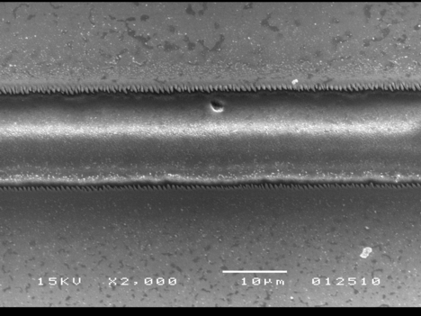 |
| This image, taken with a scanning electron microscope, shows a microchannel that was created using an ultrafast-pulsing laser.
(Purdue University School of Mechanical Engineering image/Yung Shin) |
Abstract:
High Precision Scribing of Thin Film Solar Cells by a Picosecond Laser
P.I.: Yung C. Shin, Gary Cheng (co-PI), Wenqian Hu,
Martin Yi Zhang, Seunghyun Lee
Purdue University
In this paper, the feasibility of thin-film solar cells scribing via a picosecond (ps) laser is investigated. The optical and thermal properties of thin films are studied first. Next, molybdenum and ZnO thin films are deposited on soda lime glass substrates by pulsed laser deposition. Then experiments for picosecond laser scribing are performed with different wavelengths and average powers and results are analyzed for process parameter optimization. The scribed slots are measured using a surface profilometer and a scanning electron microscope (SEM). Using the optimized laser parameters, the ablation depths of the slots are accurate within 0.1 μm tolerance, the edges are sharp without distortions and slot bottoms are flat. These slots are precisely machined with a high speed, which makes ps laser scribing of solar cells a promising technique.
Ultrafast laser 'scribing' technique to cut cost, hike efficiency of solar cells
West Lafayette, IN | Posted on March 8th, 2011Researchers are developing a technology that aims to help make solar cells more affordable and efficient by using a new manufacturing method that employs an ultrafast pulsing laser.
The innovation may help to overcome two major obstacles that hinder widespread adoption of solar cells: the need to reduce manufacturing costs and increase the efficiency of converting sunlight into an electric current, said Yung Shin, a professor of mechanical engineering and director of Purdue University's Center for Laser-Based Manufacturing.
Critical to both are tiny "microchannels" needed to interconnect a series of solar panels into an array capable of generating useable amounts of power, he said. Conventional "scribing" methods, which create the channels mechanically with a stylus, are slow and expensive and produce imperfect channels, impeding solar cells' performance.
"Production costs of solar cells have been greatly reduced by making them out of thin films instead of wafers, but it is difficult to create high-quality microchannels in these thin films," Shin said. "The mechanical scribing methods in commercial use do not create high-quality, well-defined channels. Although laser scribing has been studied extensively, until now we haven't been able to precisely control lasers to accurately create the microchannels to the exacting specifications required."
The researchers hope to increase efficiency while cutting cost significantly using an "ultrashort pulse laser" to create the microchannels in thin-film solar cells, he said.
The work, funded with a three-year, $425,000 grant from the National Science Foundation, is led by Shin and Gary Cheng, an associate professor of industrial engineering. A research paper demonstrating the feasibility of the technique was published in Proceedings of the 2011 NSF Engineering Research and Innovation Conference in January. The paper was written by Shin, Cheng, and graduate students Wenqian Hu, Martin Yi Zhang and Seunghyun Lee.
"The efficiency of solar cells depends largely on how accurate your scribing of microchannels is," Shin said. "If they are made as accurately as possibly, efficiency goes up."
Research results have shown that the fast-pulsing laser accurately formed microchannels with precise depths and sharp boundaries. The laser pulses last only a matter of picoseconds, or quadrillionths of a second. Because the pulses are so fleeting the laser does not cause heat damage to the thin film, removing material in precise patterns in a process called "cold ablation."
"It creates very clean microchannels on the surface of each layer," Shin said. "You can do this at very high speed, meters per second, which is not possible with a mechanical scribe. This is very tricky because the laser must be precisely controlled so that it penetrates only one layer of the thin film at a time, and the layers are extremely thin. You can do that with this kind of laser because you have a very precise control of the depth, to about 10 to 20 nanometers."
Traditional solar cells are usually flat and rigid, but emerging thin-film solar cells are flexible, allowing them to be used as rooftop shingles and tiles, building facades, or the glazing for skylights. Thin-film solar cells account for about 20 percent of the photovoltaic market globally in terms of watts generated and are expected to account for 31 percent by 2013.
The researchers plan to establish the scientific basis for the laser-ablation technique by the end of the three-year period. The work is funded through NSF's Civil Mechanical and Manufacturing Innovation division.
Information about photovoltaic cells is available from the U.S. Department of Energy's National Renewable Energy Laboratory at www.nrel.gov/learning/re_photovoltaics.html
####
For more information, please click here
Contacts:
Writer:
Emil Venere
765-494-4709
Sources:
Yung Shin
765-494-9775,
Gary Cheng
765-494-5436
Joshua Chamot
NSF media officer
703-292-7730
Copyright © Purdue University School of Mechanical Engineering
If you have a comment, please Contact us.Issuers of news releases, not 7th Wave, Inc. or Nanotechnology Now, are solely responsible for the accuracy of the content.
Bookmark:


| Related News Press |
News and information
![]() Decoding hydrogen‑bond network of electrolyte for cryogenic durable aqueous zinc‑ion batteries January 30th, 2026
Decoding hydrogen‑bond network of electrolyte for cryogenic durable aqueous zinc‑ion batteries January 30th, 2026
![]() COF scaffold membrane with gate‑lane nanostructure for efficient Li+/Mg2+ separation January 30th, 2026
COF scaffold membrane with gate‑lane nanostructure for efficient Li+/Mg2+ separation January 30th, 2026
![]() MXene nanomaterials enter a new dimension Multilayer nanomaterial: MXene flakes created at Drexel University show new promise as 1D scrolls January 30th, 2026
MXene nanomaterials enter a new dimension Multilayer nanomaterial: MXene flakes created at Drexel University show new promise as 1D scrolls January 30th, 2026
Imaging
![]() ICFO researchers overcome long-standing bottleneck in single photon detection with twisted 2D materials August 8th, 2025
ICFO researchers overcome long-standing bottleneck in single photon detection with twisted 2D materials August 8th, 2025
![]() Simple algorithm paired with standard imaging tool could predict failure in lithium metal batteries August 8th, 2025
Simple algorithm paired with standard imaging tool could predict failure in lithium metal batteries August 8th, 2025
Discoveries
![]() From sensors to smart systems: the rise of AI-driven photonic noses January 30th, 2026
From sensors to smart systems: the rise of AI-driven photonic noses January 30th, 2026
![]() Decoding hydrogen‑bond network of electrolyte for cryogenic durable aqueous zinc‑ion batteries January 30th, 2026
Decoding hydrogen‑bond network of electrolyte for cryogenic durable aqueous zinc‑ion batteries January 30th, 2026
![]() COF scaffold membrane with gate‑lane nanostructure for efficient Li+/Mg2+ separation January 30th, 2026
COF scaffold membrane with gate‑lane nanostructure for efficient Li+/Mg2+ separation January 30th, 2026
Announcements
![]() Decoding hydrogen‑bond network of electrolyte for cryogenic durable aqueous zinc‑ion batteries January 30th, 2026
Decoding hydrogen‑bond network of electrolyte for cryogenic durable aqueous zinc‑ion batteries January 30th, 2026
![]() COF scaffold membrane with gate‑lane nanostructure for efficient Li+/Mg2+ separation January 30th, 2026
COF scaffold membrane with gate‑lane nanostructure for efficient Li+/Mg2+ separation January 30th, 2026
Tools
![]() Metasurfaces smooth light to boost magnetic sensing precision January 30th, 2026
Metasurfaces smooth light to boost magnetic sensing precision January 30th, 2026
![]() From sensors to smart systems: the rise of AI-driven photonic noses January 30th, 2026
From sensors to smart systems: the rise of AI-driven photonic noses January 30th, 2026
![]() Japan launches fully domestically produced quantum computer: Expo visitors to experience quantum computing firsthand August 8th, 2025
Japan launches fully domestically produced quantum computer: Expo visitors to experience quantum computing firsthand August 8th, 2025
Energy
![]() Sensors innovations for smart lithium-based batteries: advancements, opportunities, and potential challenges August 8th, 2025
Sensors innovations for smart lithium-based batteries: advancements, opportunities, and potential challenges August 8th, 2025
![]() Simple algorithm paired with standard imaging tool could predict failure in lithium metal batteries August 8th, 2025
Simple algorithm paired with standard imaging tool could predict failure in lithium metal batteries August 8th, 2025
Photonics/Optics/Lasers
![]() Metasurfaces smooth light to boost magnetic sensing precision January 30th, 2026
Metasurfaces smooth light to boost magnetic sensing precision January 30th, 2026
![]() From sensors to smart systems: the rise of AI-driven photonic noses January 30th, 2026
From sensors to smart systems: the rise of AI-driven photonic noses January 30th, 2026
![]() ICFO researchers overcome long-standing bottleneck in single photon detection with twisted 2D materials August 8th, 2025
ICFO researchers overcome long-standing bottleneck in single photon detection with twisted 2D materials August 8th, 2025
Solar/Photovoltaic
![]() Spinel-type sulfide semiconductors to operate the next-generation LEDs and solar cells For solar-cell absorbers and green-LED source October 3rd, 2025
Spinel-type sulfide semiconductors to operate the next-generation LEDs and solar cells For solar-cell absorbers and green-LED source October 3rd, 2025
![]() KAIST researchers introduce new and improved, next-generation perovskite solar cell November 8th, 2024
KAIST researchers introduce new and improved, next-generation perovskite solar cell November 8th, 2024
![]() Groundbreaking precision in single-molecule optoelectronics August 16th, 2024
Groundbreaking precision in single-molecule optoelectronics August 16th, 2024
![]() Development of zinc oxide nanopagoda array photoelectrode: photoelectrochemical water-splitting hydrogen production January 12th, 2024
Development of zinc oxide nanopagoda array photoelectrode: photoelectrochemical water-splitting hydrogen production January 12th, 2024
|
|
||
|
|
||
| The latest news from around the world, FREE | ||
|
|
||
|
|
||
| Premium Products | ||
|
|
||
|
Only the news you want to read!
Learn More |
||
|
|
||
|
Full-service, expert consulting
Learn More |
||
|
|
||