Home > Press > Etched Quantum Dots Shape Up as Single Photon Emitters, NIST Tests Show
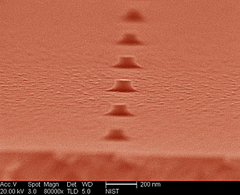 |
| Colorized micrograph of quantum dots made using electron beam lithography and etching. This type of quantum dot can be shaped and positioned more reliably than dots made with conventional crystal growth methods. Credit: Verma/NIST |
Abstract:
Like snowflakes or fingerprints, no two quantum dots are identical. But a new etching method for shaping and positioning these semiconductor nanocrystals might change that. What's more, tests at the National Institute of Standards and Technology (NIST) confirm that etched quantum dots emit single particles of light (photons), boosting prospects for powering new types of devices for quantum communications.
Etched Quantum Dots Shape Up as Single Photon Emitters, NIST Tests Show
Gaithersburg, MD | Posted on February 26th, 2011The conventional way to build quantum dots�at NIST and elsewhere�is to grow them like crystals in a solution, but this somewhat haphazard process results in irregular shapes. The new, more precise process was developed by NIST postdoctoral researcher Varun Verma when he was a student at the University of Illinois. Verma uses electron beam lithography and etching to carve quantum dots inside a semiconductor sandwich (called a quantum well) that confines particles in two dimensions. Lithography controls the dot's size and position, while sandwich thickness and composition�as well as dot size�can be used to tune the color of the dot's light emissions.
Some quantum dots are capable of emitting individual, isolated photons on demand, a crucial trait for quantum information systems that encode information by manipulating single photons. In new work reported in Optics Express,* NIST tests demonstrated that the lithographed and etched quantum dots do indeed work as sources of single photons. The tests were performed on dots made of indium gallium arsenide. Dots of various diameters were patterned in specific positions in square arrays. Using a laser to excite individual dots and a photon detector to analyze emissions, NIST researchers found that dots 35 nanometers (nm) wide, for instance, emitted nearly all light at a wavelength of 888.6 nm. The timing pattern indicated that the light was emitted as a train of single photons.
NIST researchers now plan to construct reflective cavities around individual etched dots to guide their light emissions. If each dot can emit most photons perpendicular to the chip surface, more light can be collected to make a more efficient single photon source. Vertical emission has been demonstrated with crystal-grown quantum dots, but these dots can't be positioned or distributed reliably in cavities. Etched dots offer not only precise positioning but also the possibility of making identical dots, which could be used to generate special states of light such as two or more photons that are entangled, a quantum phenomenon that links their properties even at a distance.
The quantum dots tested in the experiments were made at NIST. A final step was carried out at the University of Illinois, where a crystal layer was grown over the dots to form clean interfaces.
* V.B. Verma, M.J. Stevens, K.L. Silverman, N.L. Dias, A. Garg, J.J. Coleman and R.P. Mirin. Photon antibunching from a single lithographically defined InGaAs/GaAs quantum dot. Optics Express. Vol. 19, No. 5, Feb. 28, 2011, p. 4182. Posted online Feb. 17, 2011.
####
About NIST
The National Institute of Standards and Technology (NIST) is an agency of the U.S. Commerce Department.
For more information, please click here
Contacts:
Laura Ost
303-497-4880
Copyright © NIST
If you have a comment, please Contact us.Issuers of news releases, not 7th Wave, Inc. or Nanotechnology Now, are solely responsible for the accuracy of the content.
Bookmark:


| Related News Press |
News and information
![]() Simulating magnetization in a Heisenberg quantum spin chain April 5th, 2024
Simulating magnetization in a Heisenberg quantum spin chain April 5th, 2024
![]() NRL charters Navy�s quantum inertial navigation path to reduce drift April 5th, 2024
NRL charters Navy�s quantum inertial navigation path to reduce drift April 5th, 2024
![]() Discovery points path to flash-like memory for storing qubits: Rice find could hasten development of nonvolatile quantum memory April 5th, 2024
Discovery points path to flash-like memory for storing qubits: Rice find could hasten development of nonvolatile quantum memory April 5th, 2024
Quantum Computing
![]() Simulating magnetization in a Heisenberg quantum spin chain April 5th, 2024
Simulating magnetization in a Heisenberg quantum spin chain April 5th, 2024
![]() Discovery points path to flash-like memory for storing qubits: Rice find could hasten development of nonvolatile quantum memory April 5th, 2024
Discovery points path to flash-like memory for storing qubits: Rice find could hasten development of nonvolatile quantum memory April 5th, 2024
![]() With VECSELs towards the quantum internet Fraunhofer: IAF achieves record output power with VECSEL for quantum frequency converters April 5th, 2024
With VECSELs towards the quantum internet Fraunhofer: IAF achieves record output power with VECSEL for quantum frequency converters April 5th, 2024
![]() Chemical reactions can scramble quantum information as well as black holes April 5th, 2024
Chemical reactions can scramble quantum information as well as black holes April 5th, 2024
Discoveries
![]() Chemical reactions can scramble quantum information as well as black holes April 5th, 2024
Chemical reactions can scramble quantum information as well as black holes April 5th, 2024
![]() New micromaterial releases nanoparticles that selectively destroy cancer cells April 5th, 2024
New micromaterial releases nanoparticles that selectively destroy cancer cells April 5th, 2024
![]() Utilizing palladium for addressing contact issues of buried oxide thin film transistors April 5th, 2024
Utilizing palladium for addressing contact issues of buried oxide thin film transistors April 5th, 2024
Announcements
![]() NRL charters Navy�s quantum inertial navigation path to reduce drift April 5th, 2024
NRL charters Navy�s quantum inertial navigation path to reduce drift April 5th, 2024
![]() Discovery points path to flash-like memory for storing qubits: Rice find could hasten development of nonvolatile quantum memory April 5th, 2024
Discovery points path to flash-like memory for storing qubits: Rice find could hasten development of nonvolatile quantum memory April 5th, 2024
Quantum Dots/Rods
![]() A new kind of magnetism November 17th, 2023
A new kind of magnetism November 17th, 2023
![]() IOP Publishing celebrates World Quantum Day with the announcement of a special quantum collection and the winners of two prestigious quantum awards April 14th, 2023
IOP Publishing celebrates World Quantum Day with the announcement of a special quantum collection and the winners of two prestigious quantum awards April 14th, 2023
![]() Qubits on strong stimulants: Researchers find ways to improve the storage time of quantum information in a spin rich material January 27th, 2023
Qubits on strong stimulants: Researchers find ways to improve the storage time of quantum information in a spin rich material January 27th, 2023
![]() NIST�s grid of quantum islands could reveal secrets for powerful technologies November 18th, 2022
NIST�s grid of quantum islands could reveal secrets for powerful technologies November 18th, 2022
Quantum nanoscience
![]() Simulating magnetization in a Heisenberg quantum spin chain April 5th, 2024
Simulating magnetization in a Heisenberg quantum spin chain April 5th, 2024
![]() Optically trapped quantum droplets of light can bind together to form macroscopic complexes March 8th, 2024
Optically trapped quantum droplets of light can bind together to form macroscopic complexes March 8th, 2024
![]() Bridging light and electrons January 12th, 2024
Bridging light and electrons January 12th, 2024
![]() 'Sudden death' of quantum fluctuations defies current theories of superconductivity: Study challenges the conventional wisdom of superconducting quantum transitions January 12th, 2024
'Sudden death' of quantum fluctuations defies current theories of superconductivity: Study challenges the conventional wisdom of superconducting quantum transitions January 12th, 2024
|
|
||
|
|
||
| The latest news from around the world, FREE | ||
|
|
||
|
|
||
| Premium Products | ||
|
|
||
|
Only the news you want to read!
Learn More |
||
|
|
||
|
Full-service, expert consulting
Learn More |
||
|
|
||