Home > Press > Materials research with antiparticles: Unravelling the secret of nanocrystalline materials
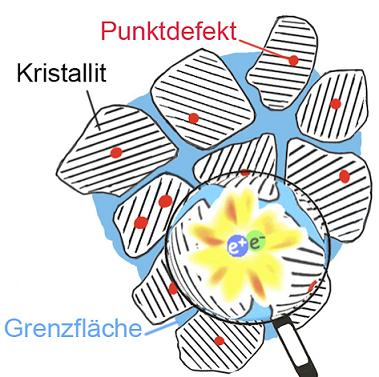 |
| Nanocrystalline materials rely on imperfection. Structural defects are responsible for their unusual material properties. Copyright Graz University of Technology |
Abstract:
Certain structural defects in materials are what make innovative nanocrystalline bulk metals very hard and yet readily malleable. As these defects are found at the atomic level of the metal structure they are difficult to investigate in experiments. However, Austrian scientists have recently taken a significant step towards understanding such atomic defects. They succeeded in doing so by combining two special methods in a project funded by the Austrian Science Fund FWF. The results have now been published in the renowned scientific journal Physical Review Letters.
Materials research with antiparticles: Unravelling the secret of nanocrystalline materials
Vienna | Posted on November 29th, 2010Extremely hard but still easily malleable - the properties of the so-called nanocrystalline bulk metals give rise to many questions among physicists. Scientists at Graz University of Technology have finally managed to answer some of those questions through experiments.
The scientists set out to monitor the structural changes in the metals in real time. They were thus able to conclude that atomic defects are a central cause of the interesting physical material properties.
Nanocrystalline metals consist of countless crystallites (grains), which are mostly smaller than one hundred nanometres - and the smaller the grain, the more solid is the metal. The structure of nanocrystalline metals is actually very regular: the atoms in the grains lie tightly packed in rank and file. However, when the metals are produced, atomic defects are involuntarily introduced which disturb the atomic order within the grains. For example, certain layers are not located directly on top of each other: some atoms are missing or rows are misaligned. Austrian materials physicists have now produced the first experimental evidence of these effects, which are closely related to the mechanical properties. They have published their results in the journal Physical Review Letters, where they describe how the combination of two special methods can be used to closely examine atomic defects.
Spy attacks on metals
As atomic defects on the nanoscale are difficult to spot, the scientists worked with so-called positrons. Dr. Wolfgang Sprengel from Graz University of Technology explains: "A positron is a subatomic particle that is almost identical to the electron, with one difference: it is positively charged. If a positron and an electron meet, they annihilate each other. In the places where atomic defects are present, there are fewer electrons and therefore fewer occurrences of annihilation. The positrons therefore serve as spies that deliver detailed information about the atomic defects. We have used this effect to analyse the fast processes of atomic defects in metals." To carry out the experiments, the scientists availed themselves of the FRM II research reactor at the Technische Universit�t M�nchen (TUM), where they deployed the positron beam with the highest intensity in the world.
Two methods, one result
In addition to the positron-electron annihilation, macroscopic length-change measurements were made upon annihilation of the defects - by means of dilatometry. This combination of dilatometry and positron-electron annihilation is a first of its kind and it delivered the evidence that some of the seemingly mysterious physical properties of the nanocrystalline bulk metals can be attributed to these structural defects. The cause of the defects can be found in the production background of the metals. Nanocrystalline bulk metals are produced using very complex methods - such as high-pressure torsion (Erich Schmidt Institute Leoben) - which give rise to the atomic defects.
The FWF project headed by Dr. Roland W�rschum is carried out in close cooperation with the University of Vienna and the Erich Schmidt Institute in Leoben, and is also closely linked to the National Research Network (NFN) on nanocrystalline bulk metals. The project has enabled a better understanding of fundamental principles, which is essential for the application of these innovative materials.
Original publikation:
In situ probing of fast defect annealing in Cu and Ni with a high-intensity positron beam. B. Oberdorfer, E-M. Steyskal, W. Sprengel, W. Puff, P. Pikart, C. Hugenschmidt, M. Zehetbauer, R. Pippan, R. W�schum. Published September 28, 2010. Physical Review Letters 105, 146101. DOI: 10.1103/PhysRevLett.105.146101.
####
For more information, please click here
Contacts:
Scientific Contact
Univ.-Prof. Dr. Roland W�rschum
Technische Universit�t Graz
Institut f�r Materialphysik
Petersgasse 16/IV
8010 Graz
T +43 / 316 / 873 - 8481
E
Austrian Science Fund FWF
Mag. Stefan Bernhardt
Haus der Forschung
Sensengasse 1
1090 Vienna, Austria
T +43 / 1 / 505 67 40 - 8111
E
Copy Editing & Distribution
PR&D � Public Relations for Research & Education
Mariannengasse 8
1090 Vienna, Austria
T +43 / 1 / 505 70 44
E
W www.prd.at
Copyright © Austrian Science Fund
If you have a comment, please Contact us.Issuers of news releases, not 7th Wave, Inc. or Nanotechnology Now, are solely responsible for the accuracy of the content.
Bookmark:


| Related News Press |
News and information
![]() Quantum computer improves AI predictions April 17th, 2026
Quantum computer improves AI predictions April 17th, 2026
![]() Flexible sensor gains sensitivity under pressure April 17th, 2026
Flexible sensor gains sensitivity under pressure April 17th, 2026
![]() A reusable chip for particulate matter sensing April 17th, 2026
A reusable chip for particulate matter sensing April 17th, 2026
![]() Detecting vibrational quantum beating in the predissociation dynamics of SF6 using time-resolved photoelectron spectroscopy April 17th, 2026
Detecting vibrational quantum beating in the predissociation dynamics of SF6 using time-resolved photoelectron spectroscopy April 17th, 2026
Govt.-Legislation/Regulation/Funding/Policy
![]() Quantum computer improves AI predictions April 17th, 2026
Quantum computer improves AI predictions April 17th, 2026
![]() Metasurfaces smooth light to boost magnetic sensing precision January 30th, 2026
Metasurfaces smooth light to boost magnetic sensing precision January 30th, 2026
![]() New imaging approach transforms study of bacterial biofilms August 8th, 2025
New imaging approach transforms study of bacterial biofilms August 8th, 2025
Academic/Education
![]() Rice University launches Rice Synthetic Biology Institute to improve lives January 12th, 2024
Rice University launches Rice Synthetic Biology Institute to improve lives January 12th, 2024
![]() Multi-institution, $4.6 million NSF grant to fund nanotechnology training September 9th, 2022
Multi-institution, $4.6 million NSF grant to fund nanotechnology training September 9th, 2022
Discoveries
![]() Quantum computer improves AI predictions April 17th, 2026
Quantum computer improves AI predictions April 17th, 2026
![]() Flexible sensor gains sensitivity under pressure April 17th, 2026
Flexible sensor gains sensitivity under pressure April 17th, 2026
![]() A reusable chip for particulate matter sensing April 17th, 2026
A reusable chip for particulate matter sensing April 17th, 2026
![]() Detecting vibrational quantum beating in the predissociation dynamics of SF6 using time-resolved photoelectron spectroscopy April 17th, 2026
Detecting vibrational quantum beating in the predissociation dynamics of SF6 using time-resolved photoelectron spectroscopy April 17th, 2026
Materials/Metamaterials/Magnetoresistance
![]() First real-time observation of two-dimensional melting process: Researchers at Mainz University unveil new insights into magnetic vortex structures August 8th, 2025
First real-time observation of two-dimensional melting process: Researchers at Mainz University unveil new insights into magnetic vortex structures August 8th, 2025
![]() Researchers unveil a groundbreaking clay-based solution to capture carbon dioxide and combat climate change June 6th, 2025
Researchers unveil a groundbreaking clay-based solution to capture carbon dioxide and combat climate change June 6th, 2025
![]() A 1960s idea inspires NBI researchers to study hitherto inaccessible quantum states June 6th, 2025
A 1960s idea inspires NBI researchers to study hitherto inaccessible quantum states June 6th, 2025
![]() Institute for Nanoscience hosts annual proposal planning meeting May 16th, 2025
Institute for Nanoscience hosts annual proposal planning meeting May 16th, 2025
Announcements
![]() A fundamentally new therapeutic approach to cystic fibrosis: Nanobody repairs cellular defect April 17th, 2026
A fundamentally new therapeutic approach to cystic fibrosis: Nanobody repairs cellular defect April 17th, 2026
![]() UC Irvine physicists discover method to reverse �quantum scrambling� : The work addresses the problem of information loss in quantum computing system April 17th, 2026
UC Irvine physicists discover method to reverse �quantum scrambling� : The work addresses the problem of information loss in quantum computing system April 17th, 2026
Tools
![]() Metasurfaces smooth light to boost magnetic sensing precision January 30th, 2026
Metasurfaces smooth light to boost magnetic sensing precision January 30th, 2026
![]() From sensors to smart systems: the rise of AI-driven photonic noses January 30th, 2026
From sensors to smart systems: the rise of AI-driven photonic noses January 30th, 2026
![]() Japan launches fully domestically produced quantum computer: Expo visitors to experience quantum computing firsthand August 8th, 2025
Japan launches fully domestically produced quantum computer: Expo visitors to experience quantum computing firsthand August 8th, 2025
Research partnerships
![]() Lab to industry: InSe wafer-scale breakthrough for future electronics August 8th, 2025
Lab to industry: InSe wafer-scale breakthrough for future electronics August 8th, 2025
![]() HKU physicists uncover hidden order in the quantum world through deconfined quantum critical points April 25th, 2025
HKU physicists uncover hidden order in the quantum world through deconfined quantum critical points April 25th, 2025
|
|
||
|
|
||
| The latest news from around the world, FREE | ||
|
|
||
|
|
||
| Premium Products | ||
|
|
||
|
Only the news you want to read!
Learn More |
||
|
|
||
|
Full-service, expert consulting
Learn More |
||
|
|
||