Home > Press > A New Twist for Nanopillar Light Collectors
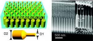 |
| On the left a schematic of a germanium nanopillar array embedded in an alumina foil membrane; on the right are cross-sectional SEM images of a blank alumina membrane with dual-diameter pores; inset shows germanium nanopillars after growth. (Images courtesy of Ali Javey) |
Abstract:
The nanopillar story has taken a new twist and the future for these materials now looks brighter than ever.
A New Twist for Nanopillar Light Collectors
Berkeley, CA | Posted on November 17th, 2010Sunlight represents the cleanest, greenest and far and away most abundant of all energy sources, and yet its potential remains woefully under-utilized. High costs have been a major deterrant to the large-scale applications of silicon-based solar cells. Nanopillars - densely packed nanoscale arrays of optically active semiconductors - have shown potential for providing a next generation of relatively cheap and scalable solar cells, but have been hampered by efficiency issues. The nanopillar story, however, has taken a new twist and the future for these materials now looks brighter than ever.
"By tuning the shape and geometry of highly ordered nanopillar arrays of germanium or cadmium sulfide, we have been able to drastically enhance the optical absorption properties of our nanopillars," says Ali Javey, a chemist who holds joint appointments with the Lawrence Berkeley National Laboratory (Berkeley Lab) and the University of California (UC) at Berkeley.
Javey, a faculty scientist with Berkeley Lab's Materials Sciences Division and a UC Berkeley professor of electrical engineering and computer science, has been at the forefront of nanopillar research. He and his group were the first to demonstrate a technique by which cadmium sulfide nanopillars can be mass-produced in large-scale flexible modules. In this latest work, they were able to produce nanopillars that absorb light as well or even better than commercial thin-film solar cells, using far less semiconductor material and without the need for anti-reflective coating.
"To enhance the broad-band optical absorption efficiency of our nanopillars we used a novel dual-diameter structure that features a small (60 nanometers) diameter tip with minimal reflectance to allow more light in, and a large (130 nanometers) diameter base for maximal absorbtion to enable more light to be converted into electricity," Javey says. "This dual-diameter structure absorbed 99-percent of incident visible light, compared to the 85 percent absorbtion by our earlier nanopillars, which had the same diameter along their entire length."
Theoretical and experimental works have shown that 3-D arrays of semiconductor nanopillars - with well-defined diameter, length and pitch - excel at trapping light while using less than half the semiconductor material required for thin-film solar cells made of compound semiconductors, such as cadmium telluride, and about one-percent of the material used in solar cells made from bulk silicon. But until the work of Javey and his research group, fabricating such nanopillars was a complex and cumbersome procedure.
Javey and his colleagues fashioned their dual diameter nanopillars from molds they made in 2.5 millimeter-thick alumina foil. A two-step anodization process was used to create an array of one micrometer deep pores in the mold with dual diameters - narrow at the top and broad at the bottom. Gold particles were then deposited into the pores to catalyze the growth of the semiconductor nanopillars.
"This process enables fine control over geometry and shape of the single-crystalline nanopillar arrays, without the use of complex epitaxial and/or lithographic processes," Javey says. "At a height of only two microns, our nanopillar arrays were able to absorb 99-percent of all photons ranging in wavelengths between 300 to 900 nanometers, without having to rely on any anti-reflective coatings."
The germanium nanopillars can be tuned to absorb infrared photons for highly sensitive detectors, and the cadmium sulfide/telluride nanopillars are ideal for solar cells. The fabrication technique is so highly generic, Javey says, it could be used with numerous other semiconductor materials as well for specific applications. Recently, he and his group demonstrated that the cross-sectional portion of the nanopillar arrays can also be tuned to assume specific shapes - square, rectangle or circle - simply by changing the shape of the template.
"This presents yet another degree of control in the optical absorption properties of nanopillars," Javey says.
Javey's dual-diameter nanopillar research was partially funded through the National Science Foundation's Center of Integrated Nanomechanical Systems (COINS) and through Berkeley Lab LDRD funds.
A paper describing this research appears on-line in the journal NANO Letters under the title "Ordered Arrays of Dual-Diameter Nanopillars for Maximized Optical Absorption." Co-authoring the paper with Javey were Zhiyong Fan, Rehan Kapadia, Paul Leu,Xiaobo Zhang, Yu-Lun Chueh, Kuniharu Takei, Kyoungsik Yu, Arash Jamshidi, Asghar Rathore, Daniel Ruebusch and Ming Wu.
For more about the research of Ali Javey, visit his Website at nano.eecs.berkeley.edu
####
About Berkeley Lab
Berkeley Lab is a U.S. Department of Energy national laboratory located in Berkeley, California. It conducts unclassified scientific research for DOE�s Office of Science and is managed by the University of California. Visit our Website at www.lbl.gov
For more information, please click here
Contacts:
Lynn Yarris
(510) 486-5375
Copyright © Berkeley Lab
If you have a comment, please Contact us.Issuers of news releases, not 7th Wave, Inc. or Nanotechnology Now, are solely responsible for the accuracy of the content.
Bookmark:


| Related News Press |
News and information
![]() Simulating magnetization in a Heisenberg quantum spin chain April 5th, 2024
Simulating magnetization in a Heisenberg quantum spin chain April 5th, 2024
![]() NRL charters Navy�s quantum inertial navigation path to reduce drift April 5th, 2024
NRL charters Navy�s quantum inertial navigation path to reduce drift April 5th, 2024
![]() Discovery points path to flash-like memory for storing qubits: Rice find could hasten development of nonvolatile quantum memory April 5th, 2024
Discovery points path to flash-like memory for storing qubits: Rice find could hasten development of nonvolatile quantum memory April 5th, 2024
![]() Good as gold - improving infectious disease testing with gold nanoparticles April 5th, 2024
Good as gold - improving infectious disease testing with gold nanoparticles April 5th, 2024
Thin films
![]() Utilizing palladium for addressing contact issues of buried oxide thin film transistors April 5th, 2024
Utilizing palladium for addressing contact issues of buried oxide thin film transistors April 5th, 2024
![]() Understanding the mechanism of non-uniform formation of diamond film on tools: Paving the way to a dry process with less environmental impact March 24th, 2023
Understanding the mechanism of non-uniform formation of diamond film on tools: Paving the way to a dry process with less environmental impact March 24th, 2023
![]() New study introduces the best graphite films: The work by Distinguished Professor Feng Ding at UNIST has been published in the October 2022 issue of Nature Nanotechnology November 4th, 2022
New study introduces the best graphite films: The work by Distinguished Professor Feng Ding at UNIST has been published in the October 2022 issue of Nature Nanotechnology November 4th, 2022
Govt.-Legislation/Regulation/Funding/Policy
![]() NRL charters Navy�s quantum inertial navigation path to reduce drift April 5th, 2024
NRL charters Navy�s quantum inertial navigation path to reduce drift April 5th, 2024
![]() Discovery points path to flash-like memory for storing qubits: Rice find could hasten development of nonvolatile quantum memory April 5th, 2024
Discovery points path to flash-like memory for storing qubits: Rice find could hasten development of nonvolatile quantum memory April 5th, 2024
![]() Chemical reactions can scramble quantum information as well as black holes April 5th, 2024
Chemical reactions can scramble quantum information as well as black holes April 5th, 2024
Possible Futures
![]() Discovery points path to flash-like memory for storing qubits: Rice find could hasten development of nonvolatile quantum memory April 5th, 2024
Discovery points path to flash-like memory for storing qubits: Rice find could hasten development of nonvolatile quantum memory April 5th, 2024
![]() With VECSELs towards the quantum internet Fraunhofer: IAF achieves record output power with VECSEL for quantum frequency converters April 5th, 2024
With VECSELs towards the quantum internet Fraunhofer: IAF achieves record output power with VECSEL for quantum frequency converters April 5th, 2024
Academic/Education
![]() Rice University launches Rice Synthetic Biology Institute to improve lives January 12th, 2024
Rice University launches Rice Synthetic Biology Institute to improve lives January 12th, 2024
![]() Multi-institution, $4.6 million NSF grant to fund nanotechnology training September 9th, 2022
Multi-institution, $4.6 million NSF grant to fund nanotechnology training September 9th, 2022
Announcements
![]() NRL charters Navy�s quantum inertial navigation path to reduce drift April 5th, 2024
NRL charters Navy�s quantum inertial navigation path to reduce drift April 5th, 2024
![]() Discovery points path to flash-like memory for storing qubits: Rice find could hasten development of nonvolatile quantum memory April 5th, 2024
Discovery points path to flash-like memory for storing qubits: Rice find could hasten development of nonvolatile quantum memory April 5th, 2024
Energy
![]() Development of zinc oxide nanopagoda array photoelectrode: photoelectrochemical water-splitting hydrogen production January 12th, 2024
Development of zinc oxide nanopagoda array photoelectrode: photoelectrochemical water-splitting hydrogen production January 12th, 2024
![]() Shedding light on unique conduction mechanisms in a new type of perovskite oxide November 17th, 2023
Shedding light on unique conduction mechanisms in a new type of perovskite oxide November 17th, 2023
![]() Inverted perovskite solar cell breaks 25% efficiency record: Researchers improve cell efficiency using a combination of molecules to address different November 17th, 2023
Inverted perovskite solar cell breaks 25% efficiency record: Researchers improve cell efficiency using a combination of molecules to address different November 17th, 2023
![]() The efficient perovskite cells with a structured anti-reflective layer � another step towards commercialization on a wider scale October 6th, 2023
The efficient perovskite cells with a structured anti-reflective layer � another step towards commercialization on a wider scale October 6th, 2023
Solar/Photovoltaic
![]() Development of zinc oxide nanopagoda array photoelectrode: photoelectrochemical water-splitting hydrogen production January 12th, 2024
Development of zinc oxide nanopagoda array photoelectrode: photoelectrochemical water-splitting hydrogen production January 12th, 2024
![]() Shedding light on unique conduction mechanisms in a new type of perovskite oxide November 17th, 2023
Shedding light on unique conduction mechanisms in a new type of perovskite oxide November 17th, 2023
![]() Inverted perovskite solar cell breaks 25% efficiency record: Researchers improve cell efficiency using a combination of molecules to address different November 17th, 2023
Inverted perovskite solar cell breaks 25% efficiency record: Researchers improve cell efficiency using a combination of molecules to address different November 17th, 2023
![]() Charged �molecular beasts� the basis for new compounds: Researchers at Leipzig University use �aggressive� fragments of molecular ions for chemical synthesis November 3rd, 2023
Charged �molecular beasts� the basis for new compounds: Researchers at Leipzig University use �aggressive� fragments of molecular ions for chemical synthesis November 3rd, 2023
|
|
||
|
|
||
| The latest news from around the world, FREE | ||
|
|
||
|
|
||
| Premium Products | ||
|
|
||
|
Only the news you want to read!
Learn More |
||
|
|
||
|
Full-service, expert consulting
Learn More |
||
|
|
||