Home > Press > Transparent Conductive Material Could Lead to Power-Generating Windows
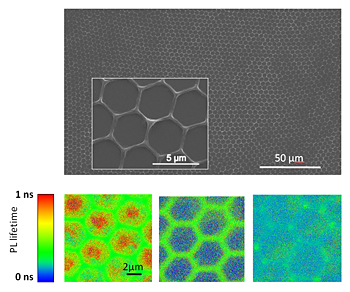 |
| Top: Scanning electron microscopy image and zoom of conjugated polymer (PPV) honeycomb. Bottom (left-to-right): Confocal fluorescence lifetime images of conjugated honeycomb, of polymer/fullerene honeycomb double layer and of polymer/fullerene honeycomb blend. Efficient charge transfer within the whole framework is observed in the case of polymer/fullerene honeycomb blend as a dramatic reduction in the fluorescence lifetime. |
Abstract:
Combines elements for light harvesting and electric charge transport over large, transparent areas
Transparent Conductive Material Could Lead to Power-Generating Windows
Upton, NY | Posted on November 3rd, 2010Scientists at the U.S. Department of Energy's (DOE) Brookhaven National Laboratory and Los Alamos National Laboratory have fabricated transparent thin films capable of absorbing light and generating electric charge over a relatively large area. The material, described in the journal Chemistry of Materials, could be used to develop transparent solar panels or even windows that absorb solar energy to generate electricity.
The material consists of a semiconducting polymer doped with carbon-rich fullerenes. Under carefully controlled conditions, the material self-assembles to form a reproducible pattern of micron-size hexagon-shaped cells over a relatively large area (up to several millimeters).
"Though such honeycomb-patterned thin films have previously been made using conventional polymers like polystyrene, this is the first report of such a material that blends semiconductors and fullerenes to absorb light and efficiently generate charge and charge separation," said lead scientist Mircea Cotlet, a physical chemist at Brookhaven's Center for Functional Nanomaterials (CFN).
Furthermore, the material remains largely transparent because the polymer chains pack densely only at the edges of the hexagons, while remaining loosely packed and spread very thin across the centers. "The densely packed edges strongly absorb light and may also facilitate conducting electricity," Cotlet explained, "while the centers do not absorb much light and are relatively transparent."
"Combining these traits and achieving large-scale patterning could enable a wide range of practical applications, such as energy-generating solar windows, transparent solar panels, and new kinds of optical displays," said co-author Zhihua Xu, a materials scientist at the CFN.
"Imagine a house with windows made of this kind of material, which, combined with a solar roof, would cut its electricity costs significantly. This is pretty exciting," Cotlet said.
The scientists fabricated the honeycomb thin films by creating a flow of micrometer-size water droplets across a thin layer of the polymer/fullerene blend solution. These water droplets self-assembled into large arrays within the polymer solution. As the solvent completely evaporates, the polymer forms a hexagonal honeycomb pattern over a large area.
"This is a cost-effective method, with potential to be scaled up from the laboratory to industrial-scale production," Xu said.
The scientists verified the uniformity of the honeycomb structure with various scanning probe and electron microscopy techniques, and tested the optical properties and charge generation at various parts of the honeycomb structure (edges, centers, and nodes where individual cells connect) using time-resolved confocal fluorescence microscopy.
The scientists also found that the degree of polymer packing was determined by the rate of solvent evaporation, which in turn determines the rate of charge transport through the material.
"The slower the solvent evaporates, the more tightly packed the polymer, and the better the charge transport," Cotlet said.
"Our work provides a deeper understanding of the optical properties of the honeycomb structure. The next step will be to use these honeycomb thin films to fabricate transparent and flexible organic solar cells and other devices," he said.
The research was supported at Los Alamos by the DOE Office of Science. The work was also carried out in part at the CFN and the Center for Integrated Nanotechnologies Gateway to Los Alamos facility. The Brookhaven team included Mircea Cotlet, Zhihua Xu, and Ranjith Krishna Pai. Collaborators from Los Alamos include Hsing-Lin Wang and Hsinhan Tsai, who are both users of the CFN facilities at Brookhaven, Andrew Dattelbaum from the Center for Integrated Nanotechnologies Gateway to Los Alamos facility, and project leader Andrew Shreve of the Materials Physics and Applications Division.
The Center for Functional Nanomaterials at Brookhaven National Laboratory and the Center for Integrated Nanotechnologies Gateway to Los Alamos facility are two of the five DOE Nanoscale Science Research Centers (NSRCs), premier national user facilities for interdisciplinary research at the nanoscale. Together the NSRCs comprise a suite of complementary facilities that provide researchers with state-of-the-art capabilities to fabricate, process, characterize and model nanoscale materials, and constitute the largest infrastructure investment of the National Nanotechnology Initiative. The NSRCs are located at DOE's Argonne, Brookhaven, Lawrence Berkeley, Oak Ridge and Sandia and Los Alamos national laboratories.
####
About Brookhaven National Laboratory
One of ten national laboratories overseen and primarily funded by the Office of Science of the U.S. Department of Energy (DOE), Brookhaven National Laboratory conducts research in the physical, biomedical, and environmental sciences, as well as in energy technologies and national security. Brookhaven Lab also builds and operates major scientific facilities available to university, industry and government researchers. Brookhaven is operated and managed for DOE's Office of Science by Brookhaven Science Associates, a limited-liability company founded by the Research Foundation of State University of New York on behalf of Stony Brook University, the largest academic user of Laboratory facilities, and Battelle, a nonprofit, applied science and technology organization.
For more information, please click here
Contacts:
Karen McNulty Walsh
(631) 344-8350
Peter Genzer
(631) 344-3174
Copyright © Brookhaven National Laboratory
If you have a comment, please Contact us.Issuers of news releases, not 7th Wave, Inc. or Nanotechnology Now, are solely responsible for the accuracy of the content.
Bookmark:


| Related News Press |
Thin films
![]() Tiny nanosheets, big leap: A new sensor detects ethanol at ultra-low levels January 30th, 2026
Tiny nanosheets, big leap: A new sensor detects ethanol at ultra-low levels January 30th, 2026
News and information
![]() Decoding hydrogen‑bond network of electrolyte for cryogenic durable aqueous zinc‑ion batteries January 30th, 2026
Decoding hydrogen‑bond network of electrolyte for cryogenic durable aqueous zinc‑ion batteries January 30th, 2026
![]() COF scaffold membrane with gate‑lane nanostructure for efficient Li+/Mg2+ separation January 30th, 2026
COF scaffold membrane with gate‑lane nanostructure for efficient Li+/Mg2+ separation January 30th, 2026
Govt.-Legislation/Regulation/Funding/Policy
![]() Metasurfaces smooth light to boost magnetic sensing precision January 30th, 2026
Metasurfaces smooth light to boost magnetic sensing precision January 30th, 2026
![]() New imaging approach transforms study of bacterial biofilms August 8th, 2025
New imaging approach transforms study of bacterial biofilms August 8th, 2025
![]() Electrifying results shed light on graphene foam as a potential material for lab grown cartilage June 6th, 2025
Electrifying results shed light on graphene foam as a potential material for lab grown cartilage June 6th, 2025
Possible Futures
![]() Decoding hydrogen‑bond network of electrolyte for cryogenic durable aqueous zinc‑ion batteries January 30th, 2026
Decoding hydrogen‑bond network of electrolyte for cryogenic durable aqueous zinc‑ion batteries January 30th, 2026
![]() COF scaffold membrane with gate‑lane nanostructure for efficient Li+/Mg2+ separation January 30th, 2026
COF scaffold membrane with gate‑lane nanostructure for efficient Li+/Mg2+ separation January 30th, 2026
Nanotubes/Buckyballs/Fullerenes/Nanorods/Nanostrings/Nanosheets
![]() Tiny nanosheets, big leap: A new sensor detects ethanol at ultra-low levels January 30th, 2026
Tiny nanosheets, big leap: A new sensor detects ethanol at ultra-low levels January 30th, 2026
![]() Enhancing power factor of p- and n-type single-walled carbon nanotubes April 25th, 2025
Enhancing power factor of p- and n-type single-walled carbon nanotubes April 25th, 2025
![]() Chainmail-like material could be the future of armor: First 2D mechanically interlocked polymer exhibits exceptional flexibility and strength January 17th, 2025
Chainmail-like material could be the future of armor: First 2D mechanically interlocked polymer exhibits exceptional flexibility and strength January 17th, 2025
![]() Innovative biomimetic superhydrophobic coating combines repair and buffering properties for superior anti-erosion December 13th, 2024
Innovative biomimetic superhydrophobic coating combines repair and buffering properties for superior anti-erosion December 13th, 2024
Announcements
![]() Decoding hydrogen‑bond network of electrolyte for cryogenic durable aqueous zinc‑ion batteries January 30th, 2026
Decoding hydrogen‑bond network of electrolyte for cryogenic durable aqueous zinc‑ion batteries January 30th, 2026
![]() COF scaffold membrane with gate‑lane nanostructure for efficient Li+/Mg2+ separation January 30th, 2026
COF scaffold membrane with gate‑lane nanostructure for efficient Li+/Mg2+ separation January 30th, 2026
Energy
![]() Sensors innovations for smart lithium-based batteries: advancements, opportunities, and potential challenges August 8th, 2025
Sensors innovations for smart lithium-based batteries: advancements, opportunities, and potential challenges August 8th, 2025
![]() Simple algorithm paired with standard imaging tool could predict failure in lithium metal batteries August 8th, 2025
Simple algorithm paired with standard imaging tool could predict failure in lithium metal batteries August 8th, 2025
Home
![]() Nanomaterials enable dual-mode heating and cooling device: Device could cut HVAC energy use by nearly 20% in the US December 2nd, 2020
Nanomaterials enable dual-mode heating and cooling device: Device could cut HVAC energy use by nearly 20% in the US December 2nd, 2020
![]() Bosch Sensortec launches ideation community to foster and accelerate innovative IoT applications : Creativity hub for customers, partners, developers and makers February 18th, 2019
Bosch Sensortec launches ideation community to foster and accelerate innovative IoT applications : Creativity hub for customers, partners, developers and makers February 18th, 2019
![]() Iran Develops Water-Repellent Nano-Paint December 5th, 2018
Iran Develops Water-Repellent Nano-Paint December 5th, 2018
Solar/Photovoltaic
![]() Spinel-type sulfide semiconductors to operate the next-generation LEDs and solar cells For solar-cell absorbers and green-LED source October 3rd, 2025
Spinel-type sulfide semiconductors to operate the next-generation LEDs and solar cells For solar-cell absorbers and green-LED source October 3rd, 2025
![]() KAIST researchers introduce new and improved, next-generation perovskite solar cell November 8th, 2024
KAIST researchers introduce new and improved, next-generation perovskite solar cell November 8th, 2024
![]() Groundbreaking precision in single-molecule optoelectronics August 16th, 2024
Groundbreaking precision in single-molecule optoelectronics August 16th, 2024
![]() Development of zinc oxide nanopagoda array photoelectrode: photoelectrochemical water-splitting hydrogen production January 12th, 2024
Development of zinc oxide nanopagoda array photoelectrode: photoelectrochemical water-splitting hydrogen production January 12th, 2024
|
|
||
|
|
||
| The latest news from around the world, FREE | ||
|
|
||
|
|
||
| Premium Products | ||
|
|
||
|
Only the news you want to read!
Learn More |
||
|
|
||
|
Full-service, expert consulting
Learn More |
||
|
|
||