Home > Press > Single-crystal films could advance solar cells
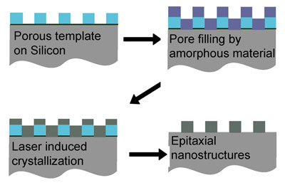 |
| Amorphous silicon, deposited on a porous template fills the empty spaces. Laser heating melts the deposit and the top few microns of the silicon substrate. In a few nanoseconds the melted silicon recrystallizes. The substrate acts as a seed crystal for the material above, causing it to crystallize with the same alignment. This makes it easier for electric charges to flow, making possible more efficient solar cells and batteries. Provided/Wiesner lab |
Abstract:
Cornell researchers have developed a new method to create a patterned single-crystal thin film of semiconductor material that could lead to more efficient photovoltaic cells and batteries.
By Bill Steele
Single-crystal films could advance solar cells
Ithaca, NY | Posted on October 8th, 2010The "holy grail" for such applications has been to create on a silicon base, or substrate, a film with a 3-D structure at the nanoscale, with the crystal lattice of the film aligned in the same direction (epitaxially) as in the substrate. Doing so is the culmination of years of research by Uli Wiesner, professor of materials science and engineering, into using polymer chemistry to create nanoscale self-assembling structures.
He and his colleagues report the breakthrough in the Oct. 8 issue of the journal Science. They used the new method to create a film with a raised texture, made up of tiny pillars just a few nanometers across. "Just the ability to make a single-crystal nanostructure has a lot of promise," Wiesner said. "We combine that with the ability of organic polymer materials to self-assemble at the nanoscale into various structures that can be templated into the crystalline material." (A nanometer -- nm -- is a billionth of a meter, about three atoms wide.)
Wiesner's research group previously used self-assembly techniques to create Gr�etzel solar cells, which use an organic dye sandwiched between two conductors. Arranging the conductors in a complex 3-D pattern creates more surface area to collect light and allows more efficient charge transport, Wiesner said.
Performance improves the most when the conducting materials are single crystals, Wiesner said. Most techniques for creating such films produce polycrystalline material -- a collection of "grains" or small crystals bunched together at random -- and grain boundaries retard the movement of electric charges, he explained.
Wiesner's method uses block co-polymers to create porous templates into which a new material can flow and crystallize. A polymer consists of organic molecules that link into long chains to form a solid. A block co-polymer is made by joining two different molecules at their ends. When they chain together and are mixed with metal oxides, one forms a nanoscale pattern of repeating geometric shapes, while the other fills the space in between. Burning the polymer away leaves a porous metal oxide nanostructure that can act as a template.
Wiesner's team created a template with hexagonal pores on a silicon single-crystal substrate and deposited films of amorphous silicon or nickel silicide over it. In collaboration with Mike Thompson, associate professor of materials science and engineering, they then heated the silicon surface with very short (nanosecond) laser pulses. This melts the newly deposited layer and the top few microns (millionths of a meter) of the silicon substrate. After only a few tens of nanoseconds the molten silicon recrystallizes with the single crystal silicon substrate acting as a seed crystal to trigger crystallization in the deposited material above it, causing that crystal to line up epitaxially with the seed.
The template is dissolved away, leaving an array of hexagonal pillars about 30 nm across. The team has made porous nanostructured films up to 100 nm thick with other complex shapes. In previous work Wiesner created lattices of cylinders, planes, spheres and complex "gyroids" by varying the composition of co-polymers.
Other materials could be deposited, the researchers said. The goal here, they said, was to demonstrate the formation of film with the same material as the substrate (officially known as homoepitaxy) and with a different material (heteroepitaxy).
In a further proof-of-concept experiment, the researchers showed that the structured thin film could be arranged in micron-scale patterns, as might be necessary in designing an electronic circuit, by laying a mask over the surface before applying laser heating.
"We have essentially gotten to the holy grail," Wiesner said. "It is not only a nanostructured single crystal, but it has an epitaxial relation to the substrate. There is no better control."
The research was supported by the National Science Foundation, Department of Homeland Security and Cornell's Energy Materials Center, funded by the U.S. Department of Energy.
####
For more information, please click here
Contacts:
Media Contact:
Joe Schwartz
(607) 254-6235
Cornell Chronicle:
Bill Steele
(607) 255-7164
Copyright © Cornell University
If you have a comment, please Contact us.Issuers of news releases, not 7th Wave, Inc. or Nanotechnology Now, are solely responsible for the accuracy of the content.
Bookmark:


| Related News Press |
Thin films
![]() Tiny nanosheets, big leap: A new sensor detects ethanol at ultra-low levels January 30th, 2026
Tiny nanosheets, big leap: A new sensor detects ethanol at ultra-low levels January 30th, 2026
![]() Utilizing palladium for addressing contact issues of buried oxide thin film transistors April 5th, 2024
Utilizing palladium for addressing contact issues of buried oxide thin film transistors April 5th, 2024
![]() Understanding the mechanism of non-uniform formation of diamond film on tools: Paving the way to a dry process with less environmental impact March 24th, 2023
Understanding the mechanism of non-uniform formation of diamond film on tools: Paving the way to a dry process with less environmental impact March 24th, 2023
News and information
![]() Decoding hydrogen‑bond network of electrolyte for cryogenic durable aqueous zinc‑ion batteries January 30th, 2026
Decoding hydrogen‑bond network of electrolyte for cryogenic durable aqueous zinc‑ion batteries January 30th, 2026
![]() COF scaffold membrane with gate‑lane nanostructure for efficient Li+/Mg2+ separation January 30th, 2026
COF scaffold membrane with gate‑lane nanostructure for efficient Li+/Mg2+ separation January 30th, 2026
Videos/Movies
![]() ICFO researchers overcome long-standing bottleneck in single photon detection with twisted 2D materials August 8th, 2025
ICFO researchers overcome long-standing bottleneck in single photon detection with twisted 2D materials August 8th, 2025
![]() New X-ray imaging technique to study the transient phases of quantum materials December 29th, 2022
New X-ray imaging technique to study the transient phases of quantum materials December 29th, 2022
Govt.-Legislation/Regulation/Funding/Policy
![]() Metasurfaces smooth light to boost magnetic sensing precision January 30th, 2026
Metasurfaces smooth light to boost magnetic sensing precision January 30th, 2026
![]() New imaging approach transforms study of bacterial biofilms August 8th, 2025
New imaging approach transforms study of bacterial biofilms August 8th, 2025
![]() Electrifying results shed light on graphene foam as a potential material for lab grown cartilage June 6th, 2025
Electrifying results shed light on graphene foam as a potential material for lab grown cartilage June 6th, 2025
Possible Futures
![]() Decoding hydrogen‑bond network of electrolyte for cryogenic durable aqueous zinc‑ion batteries January 30th, 2026
Decoding hydrogen‑bond network of electrolyte for cryogenic durable aqueous zinc‑ion batteries January 30th, 2026
![]() COF scaffold membrane with gate‑lane nanostructure for efficient Li+/Mg2+ separation January 30th, 2026
COF scaffold membrane with gate‑lane nanostructure for efficient Li+/Mg2+ separation January 30th, 2026
Academic/Education
![]() Rice University launches Rice Synthetic Biology Institute to improve lives January 12th, 2024
Rice University launches Rice Synthetic Biology Institute to improve lives January 12th, 2024
![]() Multi-institution, $4.6 million NSF grant to fund nanotechnology training September 9th, 2022
Multi-institution, $4.6 million NSF grant to fund nanotechnology training September 9th, 2022
Self Assembly
![]() Diamond glitter: A play of colors with artificial DNA crystals May 17th, 2024
Diamond glitter: A play of colors with artificial DNA crystals May 17th, 2024
![]() Liquid crystal templated chiral nanomaterials October 14th, 2022
Liquid crystal templated chiral nanomaterials October 14th, 2022
![]() Nanoclusters self-organize into centimeter-scale hierarchical assemblies April 22nd, 2022
Nanoclusters self-organize into centimeter-scale hierarchical assemblies April 22nd, 2022
![]() Atom by atom: building precise smaller nanoparticles with templates March 4th, 2022
Atom by atom: building precise smaller nanoparticles with templates March 4th, 2022
Announcements
![]() Decoding hydrogen‑bond network of electrolyte for cryogenic durable aqueous zinc‑ion batteries January 30th, 2026
Decoding hydrogen‑bond network of electrolyte for cryogenic durable aqueous zinc‑ion batteries January 30th, 2026
![]() COF scaffold membrane with gate‑lane nanostructure for efficient Li+/Mg2+ separation January 30th, 2026
COF scaffold membrane with gate‑lane nanostructure for efficient Li+/Mg2+ separation January 30th, 2026
Energy
![]() Sensors innovations for smart lithium-based batteries: advancements, opportunities, and potential challenges August 8th, 2025
Sensors innovations for smart lithium-based batteries: advancements, opportunities, and potential challenges August 8th, 2025
![]() Simple algorithm paired with standard imaging tool could predict failure in lithium metal batteries August 8th, 2025
Simple algorithm paired with standard imaging tool could predict failure in lithium metal batteries August 8th, 2025
Battery Technology/Capacitors/Generators/Piezoelectrics/Thermoelectrics/Energy storage
![]() Decoding hydrogen‑bond network of electrolyte for cryogenic durable aqueous zinc‑ion batteries January 30th, 2026
Decoding hydrogen‑bond network of electrolyte for cryogenic durable aqueous zinc‑ion batteries January 30th, 2026
![]() COF scaffold membrane with gate‑lane nanostructure for efficient Li+/Mg2+ separation January 30th, 2026
COF scaffold membrane with gate‑lane nanostructure for efficient Li+/Mg2+ separation January 30th, 2026
![]() MXene nanomaterials enter a new dimension Multilayer nanomaterial: MXene flakes created at Drexel University show new promise as 1D scrolls January 30th, 2026
MXene nanomaterials enter a new dimension Multilayer nanomaterial: MXene flakes created at Drexel University show new promise as 1D scrolls January 30th, 2026
Solar/Photovoltaic
![]() Spinel-type sulfide semiconductors to operate the next-generation LEDs and solar cells For solar-cell absorbers and green-LED source October 3rd, 2025
Spinel-type sulfide semiconductors to operate the next-generation LEDs and solar cells For solar-cell absorbers and green-LED source October 3rd, 2025
![]() KAIST researchers introduce new and improved, next-generation perovskite solar cell November 8th, 2024
KAIST researchers introduce new and improved, next-generation perovskite solar cell November 8th, 2024
![]() Groundbreaking precision in single-molecule optoelectronics August 16th, 2024
Groundbreaking precision in single-molecule optoelectronics August 16th, 2024
![]() Development of zinc oxide nanopagoda array photoelectrode: photoelectrochemical water-splitting hydrogen production January 12th, 2024
Development of zinc oxide nanopagoda array photoelectrode: photoelectrochemical water-splitting hydrogen production January 12th, 2024
|
|
||
|
|
||
| The latest news from around the world, FREE | ||
|
|
||
|
|
||
| Premium Products | ||
|
|
||
|
Only the news you want to read!
Learn More |
||
|
|
||
|
Full-service, expert consulting
Learn More |
||
|
|
||