Home > Press > Novelda AS to Exhibit Nanoscale Impulse Radar at EXPO 2010 in Shanghai, China
 |
Abstract:
Novelda AS, a fabless semiconductor company specializing in nanoscale wireless low-power technology for impulse radar, has been invited by the Norwegian government and Innovation Norway to exhibit at the prestigious EXPO 2010, taking place in Shanghai, China in September 2010.
Novelda AS to Exhibit Nanoscale Impulse Radar at EXPO 2010 in Shanghai, China
Oslo, Norway | Posted on September 6th, 2010"Our impulse radar technology is being evaluated and used by companies around the globe, in a wide variety of applications," says Aage Kalsaeg, Novelda's Chief Marketing Officer. "Participation in the EXPO 2010 exhibition will strengthen our momentum since introducing this technology in Q3 2009."
"Our low-power CMOS transceiver, with its near field operation, ultra-high resolution, allows the Novelda technology to be used in diverse applications such as human vital sign monitoring, personal security, environmental monitoring, industrial automation and other novel sensor applications," said Mr. Kalsaeg.
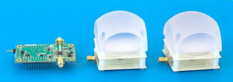
The NVA6000 range of impulse-based radar chips provides an exciting and innovative solution to many sensor applications. Novelda Nanoscale Impulse Radar emits electromagnetic (EM) pulses and then measures the backscattered (reflected) energy from objects in the surroundings. As radio waves have penetrating properties, reflections from hidden objects like the heart in the human body or objects behind an obstacle can be detected due to the receivers' ultra-high sensitivity.
The Novelda Impulse Radar is a complete CMOS radar transceiver integrated on a single chip. The high bandwidth of the transmitted pulses offers unique penetration abilities and very high accuracy. The core technology of the Novelda impulse radar technology requires no clock, yielding higher speed and lower power.
Novelda radar chips can both complement or replace existing technologies such as video, ultrasound and infrared sensors. Many new applications are now possible due to its speed, resolution, and its ability to "see through" obstacles. Lenses no longer need to be cleaned, thus the cost of ownership can be dramatically reduced compared to technologies requiring free visibility. Since the NVA6000-series chips are single-chip transceivers, they are also suitable for integration into small and mobile devices.
Novelda provides development kits and software for all available chips to help developers save time and cost for prototyping and concept development.
####
About Novelda AS
Novelda AS is a privately held, R&D driven, fabless semiconductor company based in Norway specializing in nanoscale wireless low-power technology for ultra-high resolution impulse radar.
Novelda was founded in 2004 as a technology spin-out from the University in Oslo, and there remains a strong Research & Development partnership with the University.
Novelda will also exhibit at the ICUWB 2010 in Nanjing, China on September 20-23, 2010: www.emfield.org/icuwb2010/
For more information, please click here
Copyright © PrNewswire
If you have a comment, please Contact us.Issuers of news releases, not 7th Wave, Inc. or Nanotechnology Now, are solely responsible for the accuracy of the content.
Bookmark:


| Related News Press |
News and information
![]() Decoding hydrogen‑bond network of electrolyte for cryogenic durable aqueous zinc‑ion batteries January 30th, 2026
Decoding hydrogen‑bond network of electrolyte for cryogenic durable aqueous zinc‑ion batteries January 30th, 2026
![]() COF scaffold membrane with gate‑lane nanostructure for efficient Li+/Mg2+ separation January 30th, 2026
COF scaffold membrane with gate‑lane nanostructure for efficient Li+/Mg2+ separation January 30th, 2026
Nanomedicine
![]() New molecular technology targets tumors and simultaneously silences two �undruggable� cancer genes August 8th, 2025
New molecular technology targets tumors and simultaneously silences two �undruggable� cancer genes August 8th, 2025
![]() New imaging approach transforms study of bacterial biofilms August 8th, 2025
New imaging approach transforms study of bacterial biofilms August 8th, 2025
![]() Cambridge chemists discover simple way to build bigger molecules � one carbon at a time June 6th, 2025
Cambridge chemists discover simple way to build bigger molecules � one carbon at a time June 6th, 2025
![]() Electrifying results shed light on graphene foam as a potential material for lab grown cartilage June 6th, 2025
Electrifying results shed light on graphene foam as a potential material for lab grown cartilage June 6th, 2025
Sensors
![]() Tiny nanosheets, big leap: A new sensor detects ethanol at ultra-low levels January 30th, 2026
Tiny nanosheets, big leap: A new sensor detects ethanol at ultra-low levels January 30th, 2026
![]() From sensors to smart systems: the rise of AI-driven photonic noses January 30th, 2026
From sensors to smart systems: the rise of AI-driven photonic noses January 30th, 2026
![]() Sensors innovations for smart lithium-based batteries: advancements, opportunities, and potential challenges August 8th, 2025
Sensors innovations for smart lithium-based batteries: advancements, opportunities, and potential challenges August 8th, 2025
Announcements
![]() Decoding hydrogen‑bond network of electrolyte for cryogenic durable aqueous zinc‑ion batteries January 30th, 2026
Decoding hydrogen‑bond network of electrolyte for cryogenic durable aqueous zinc‑ion batteries January 30th, 2026
![]() COF scaffold membrane with gate‑lane nanostructure for efficient Li+/Mg2+ separation January 30th, 2026
COF scaffold membrane with gate‑lane nanostructure for efficient Li+/Mg2+ separation January 30th, 2026
Tools
![]() Metasurfaces smooth light to boost magnetic sensing precision January 30th, 2026
Metasurfaces smooth light to boost magnetic sensing precision January 30th, 2026
![]() From sensors to smart systems: the rise of AI-driven photonic noses January 30th, 2026
From sensors to smart systems: the rise of AI-driven photonic noses January 30th, 2026
![]() Japan launches fully domestically produced quantum computer: Expo visitors to experience quantum computing firsthand August 8th, 2025
Japan launches fully domestically produced quantum computer: Expo visitors to experience quantum computing firsthand August 8th, 2025
Environment
![]() Researchers unveil a groundbreaking clay-based solution to capture carbon dioxide and combat climate change June 6th, 2025
Researchers unveil a groundbreaking clay-based solution to capture carbon dioxide and combat climate change June 6th, 2025
![]() Onion-like nanoparticles found in aircraft exhaust May 14th, 2025
Onion-like nanoparticles found in aircraft exhaust May 14th, 2025
Events/Classes
![]() Institute for Nanoscience hosts annual proposal planning meeting May 16th, 2025
Institute for Nanoscience hosts annual proposal planning meeting May 16th, 2025
![]() A New Blue: Mysterious origin of the ribbontail ray�s electric blue spots revealed July 5th, 2024
A New Blue: Mysterious origin of the ribbontail ray�s electric blue spots revealed July 5th, 2024
![]() Researchers demonstrate co-propagation of quantum and classical signals: Study shows that quantum encryption can be implemented in existing fiber networks January 20th, 2023
Researchers demonstrate co-propagation of quantum and classical signals: Study shows that quantum encryption can be implemented in existing fiber networks January 20th, 2023
|
|
||
|
|
||
| The latest news from around the world, FREE | ||
|
|
||
|
|
||
| Premium Products | ||
|
|
||
|
Only the news you want to read!
Learn More |
||
|
|
||
|
Full-service, expert consulting
Learn More |
||
|
|
||