Home > Press > New Microscope Features Ultra Stable Specimen Stage For High Magnification Navigation
 |
Abstract:
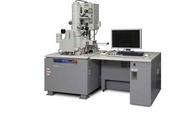
The new SU8040 Field Emission Scanning Electron Microscope (FE-SEM) from Hitachi High-Technologies features a newly developed Regulus (REGULated Ultra Stable) Specimen Stage for unprecedented smooth sample control even at ultra-high magnification.
New Microscope Features Ultra Stable Specimen Stage For High Magnification Navigation
UK | Posted on August 31st, 2010The SU8040 is an outstanding tool for the leading nanotechnology industries, such as the semiconductor industry and cutting-edge nanotechnology material analysis.
Nanotechnology and semiconductor samples contain structures of nanometre dimensions which need to be imaged and measured at hundreds of thousand times magnification and ultra high resolution. The Regulus stage provides the extremely fine specimen stage control that is needed for smooth operation at such high magnifications in order to be able to locate and maintain the regions of interest. The Regulus stage uses a proven conventional motor drive with a newly developed motor drivetrain to give seamless stage operation throughout the magnification range.
Also new for the SU8040 is the optional �cell count assist' software. This software recognises the repeat patterns of DRAM/SRAM samples, and makes use of the outstanding Regulus stage performance to allow automated identification of patterns for measurement and defect analysis. The automated approach eliminates tedious manual searching for the regions of interest.
The SU8040 offers outstanding imaging capabilities, with a resolution capability of 1.3nm at a landing voltage of 1.0kV. The SU8040 benefits from Hitachi's revolutionary in-lens triple detection system, originally introduced on the SU8000. This novel, ultra-sensitive detection system allows high efficiency simultaneous multi-signal imaging and energy filtering. The extraordinary versatility of this detection system not only provides high sensitivity detection for ultra-low current imaging of sensitive materials, but also allows the imaging of structures and surface properties never seen before - taking SEM imaging into whole new areas of materials examination and development.
Secondary electrons, low angle and high angle backscattered electrons can be detected and displayed either independently or as a mixed signal image using a primary beam of as little as 100v, providing the capability to observe the absolute surface structure as well as properties such as surface potential contrast.
####
For more information, please click here
Contacts:
Press Contact:
Denis Bulgin
Tel: +44 1763 262621
Other Enquiries:
Hitachi High-Technologies Corporation, Whitebrook Park, Lower Cookham Road,
Maidenhead, Berkshire UK, SL6 8YA. Tel: + 44 (0) 800 316 1500.
Copyright © Hitachi High-Technologies
If you have a comment, please Contact us.Issuers of news releases, not 7th Wave, Inc. or Nanotechnology Now, are solely responsible for the accuracy of the content.
Bookmark:


| Related News Press |
News and information
![]() Quantum computer improves AI predictions April 17th, 2026
Quantum computer improves AI predictions April 17th, 2026
![]() Flexible sensor gains sensitivity under pressure April 17th, 2026
Flexible sensor gains sensitivity under pressure April 17th, 2026
![]() A reusable chip for particulate matter sensing April 17th, 2026
A reusable chip for particulate matter sensing April 17th, 2026
![]() Detecting vibrational quantum beating in the predissociation dynamics of SF6 using time-resolved photoelectron spectroscopy April 17th, 2026
Detecting vibrational quantum beating in the predissociation dynamics of SF6 using time-resolved photoelectron spectroscopy April 17th, 2026
Announcements
![]() A fundamentally new therapeutic approach to cystic fibrosis: Nanobody repairs cellular defect April 17th, 2026
A fundamentally new therapeutic approach to cystic fibrosis: Nanobody repairs cellular defect April 17th, 2026
![]() UC Irvine physicists discover method to reverse �quantum scrambling� : The work addresses the problem of information loss in quantum computing system April 17th, 2026
UC Irvine physicists discover method to reverse �quantum scrambling� : The work addresses the problem of information loss in quantum computing system April 17th, 2026
Tools
![]() Metasurfaces smooth light to boost magnetic sensing precision January 30th, 2026
Metasurfaces smooth light to boost magnetic sensing precision January 30th, 2026
![]() From sensors to smart systems: the rise of AI-driven photonic noses January 30th, 2026
From sensors to smart systems: the rise of AI-driven photonic noses January 30th, 2026
![]() Japan launches fully domestically produced quantum computer: Expo visitors to experience quantum computing firsthand August 8th, 2025
Japan launches fully domestically produced quantum computer: Expo visitors to experience quantum computing firsthand August 8th, 2025
|
|
||
|
|
||
| The latest news from around the world, FREE | ||
|
|
||
|
|
||
| Premium Products | ||
|
|
||
|
Only the news you want to read!
Learn More |
||
|
|
||
|
Full-service, expert consulting
Learn More |
||
|
|
||