Home > Press > Designer optoelectronics – quantum mechanics for new materials
 |
Abstract:
European researchers have combined computer modelling of quantum mechanics and precision fabrication processes to create novel transparent conductive oxides made to order for a wide range of scientific and consumer applications.
Designer optoelectronics – quantum mechanics for new materials
EU | Posted on August 30th, 2010Imagine specifying exactly how you want a new material to behave, handing those specs to an engineer, and getting back a brand-new material with exactly the qualities you need.
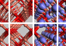
That's what the EU-funded project NATCO (for Novel Advanced Transparent Conductive Oxides) set out to do. They designed and developed novel transparent conductive oxides (TCOs) to exacting specifications by applying quantum mechanics to predict a material's optical and electronic properties, fabricating it, and checking their results experimentally.
The results? Completely new TCOs with a wide range of potential applications in sensors, solar cells, smart windows, and dozens of other scientific, commercial and consumer products.
"In the field of optoelectronics, there's a great need to find better and less costly materials," says Guy Garry, coordinator of the NATCO project. "The route we took was first to make calculations to find the best way to get the properties that we needed. When we fabricated these materials, we found that their properties were the same as we had calculated."
This rational design process - using first principles to calculate the conductivity and transparency of novel materials before fabricating them - allowed the researchers to develop new TCOs with enhanced performance rapidly and efficiently.
"We were able to make these calculations very quickly, which allowed us to enhance existing properties and find new properties," says Dr Garry.
Brand new optoelectronic material
TCOs - materials that combine transparency and conductivity, qualities that are not usually found together - have multiple applications. As sensors, photovoltaics, light emitting devices and electronically controllable films, they are found in scientific instruments, DVDs, digital cameras, mobile phones, computer displays and hundreds of other products.
Until recently, most TCOs relied on a material called ITO, an oxide of indium which is doped - slightly modified - by the addition of a small quantity of tin. ITOs have proved useful, but, Dr Garry says, suffer from two drawbacks. Their transparency is not very good, especially in the near-infrared range, and indium is in short supply and very expensive.
The NATCO team decided to explore a completely different material, strontium cuprate doped with varying amounts of barium. Copper, barium and strontium are far more abundant and much less expensive than indium.
Extensive calculations applying quantum mechanics predicted that, by doping strontium cuprate with a few percent by weight of barium, the researchers could create precisely the materials they wanted, combining good electrical conductivity and optical transparency.
Fabricating the new materials was a challenge. At first the materials were fabricated in the form of bulk ceramics and then, for actual applications, thin layers were deposited on suitable substrates.
In the end, the researchers settled on two deposition techniques - pulsed laser deposition (PLD) and metal organic chemical deposition (MOCVD).
In PLD, a burst of laser light vaporises the material to be deposited, creating a thin film on a glass or silicon surface. It allows precise control, but can't be used on large surfaces.
MOCVD uses organic chemistry to create gasses that deposit the desired material onto a surface. It is a more complicated procedure, but has the advantage of being able to be scaled up to coat large surfaces.
Once they had fabricated the materials, the researchers could test how well their electrical and optical properties matched the predicted values. "This was the first time that this kind of work was done on TCOs," says Dr Garry.
Multiple applications in the works
Today, one of the most promising applications of NATCO's new TCOs is in the area of exquisitely sensitive biosensors. These devices, with the tongue-twisting title of Elecro-Chemical Optical Waveguide Light-mode Spectroscopy Sensors, are fabricated by the Hungarian consortium partner MicroVacuum. They work by measuring how light is bent as it passes through a very thin optical wave guiding layer.
When target molecules bind to the surface of the detector, they change the TCO´s refractive index, which in turn changes how light passes through the waveguide. Applying a varying electric field through the layer provides further information about the molecules.
"We got very good results on these devices using our strontium cuprate materials," says Dr Garry. He foresees a wide range of applications for these sensors, especially in the area of proteomics.
The project's commercial and academic partners are pursuing other applications for NATCO's designer TCOs, including more efficient solar cells, smart windows, novel light sources, and materials to modulate laser light.
For Dr Garry, the results of the project's first-principles modelling and precision fabrication approach are so encouraging that he plans to apply them to more challenging problems.
"We'd like to use this route to study more complicated materials," he says. "For example, to look at ferro-electricity to see why some materials with the same structure are ferro-electric while others are not."
The NATCO project received funding from the FET-Open strand of the EU's Sixth Framework Programme for research.
####
For more information, please click here
Copyright © ITC Results
If you have a comment, please Contact us.Issuers of news releases, not 7th Wave, Inc. or Nanotechnology Now, are solely responsible for the accuracy of the content.
Bookmark:


| Related News Press |
News and information
![]() Quantum computer improves AI predictions April 17th, 2026
Quantum computer improves AI predictions April 17th, 2026
![]() Flexible sensor gains sensitivity under pressure April 17th, 2026
Flexible sensor gains sensitivity under pressure April 17th, 2026
![]() A reusable chip for particulate matter sensing April 17th, 2026
A reusable chip for particulate matter sensing April 17th, 2026
![]() Detecting vibrational quantum beating in the predissociation dynamics of SF6 using time-resolved photoelectron spectroscopy April 17th, 2026
Detecting vibrational quantum beating in the predissociation dynamics of SF6 using time-resolved photoelectron spectroscopy April 17th, 2026
Govt.-Legislation/Regulation/Funding/Policy
![]() Quantum computer improves AI predictions April 17th, 2026
Quantum computer improves AI predictions April 17th, 2026
![]() Metasurfaces smooth light to boost magnetic sensing precision January 30th, 2026
Metasurfaces smooth light to boost magnetic sensing precision January 30th, 2026
![]() New imaging approach transforms study of bacterial biofilms August 8th, 2025
New imaging approach transforms study of bacterial biofilms August 8th, 2025
Possible Futures
![]() A fundamentally new therapeutic approach to cystic fibrosis: Nanobody repairs cellular defect April 17th, 2026
A fundamentally new therapeutic approach to cystic fibrosis: Nanobody repairs cellular defect April 17th, 2026
![]() UC Irvine physicists discover method to reverse ‘quantum scrambling’ : The work addresses the problem of information loss in quantum computing system April 17th, 2026
UC Irvine physicists discover method to reverse ‘quantum scrambling’ : The work addresses the problem of information loss in quantum computing system April 17th, 2026
Sensors
![]() Flexible sensor gains sensitivity under pressure April 17th, 2026
Flexible sensor gains sensitivity under pressure April 17th, 2026
![]() Tiny nanosheets, big leap: A new sensor detects ethanol at ultra-low levels January 30th, 2026
Tiny nanosheets, big leap: A new sensor detects ethanol at ultra-low levels January 30th, 2026
![]() From sensors to smart systems: the rise of AI-driven photonic noses January 30th, 2026
From sensors to smart systems: the rise of AI-driven photonic noses January 30th, 2026
![]() Sensors innovations for smart lithium-based batteries: advancements, opportunities, and potential challenges August 8th, 2025
Sensors innovations for smart lithium-based batteries: advancements, opportunities, and potential challenges August 8th, 2025
Announcements
![]() A fundamentally new therapeutic approach to cystic fibrosis: Nanobody repairs cellular defect April 17th, 2026
A fundamentally new therapeutic approach to cystic fibrosis: Nanobody repairs cellular defect April 17th, 2026
![]() UC Irvine physicists discover method to reverse ‘quantum scrambling’ : The work addresses the problem of information loss in quantum computing system April 17th, 2026
UC Irvine physicists discover method to reverse ‘quantum scrambling’ : The work addresses the problem of information loss in quantum computing system April 17th, 2026
Solar/Photovoltaic
![]() Spinel-type sulfide semiconductors to operate the next-generation LEDs and solar cells For solar-cell absorbers and green-LED source October 3rd, 2025
Spinel-type sulfide semiconductors to operate the next-generation LEDs and solar cells For solar-cell absorbers and green-LED source October 3rd, 2025
![]() KAIST researchers introduce new and improved, next-generation perovskite solar cell November 8th, 2024
KAIST researchers introduce new and improved, next-generation perovskite solar cell November 8th, 2024
![]() Groundbreaking precision in single-molecule optoelectronics August 16th, 2024
Groundbreaking precision in single-molecule optoelectronics August 16th, 2024
![]() Development of zinc oxide nanopagoda array photoelectrode: photoelectrochemical water-splitting hydrogen production January 12th, 2024
Development of zinc oxide nanopagoda array photoelectrode: photoelectrochemical water-splitting hydrogen production January 12th, 2024
Quantum nanoscience
![]() Beyond silicon: Electronics at the scale of a single molecule January 30th, 2026
Beyond silicon: Electronics at the scale of a single molecule January 30th, 2026
![]() MXene nanomaterials enter a new dimension Multilayer nanomaterial: MXene flakes created at Drexel University show new promise as 1D scrolls January 30th, 2026
MXene nanomaterials enter a new dimension Multilayer nanomaterial: MXene flakes created at Drexel University show new promise as 1D scrolls January 30th, 2026
![]() ICFO researchers overcome long-standing bottleneck in single photon detection with twisted 2D materials August 8th, 2025
ICFO researchers overcome long-standing bottleneck in single photon detection with twisted 2D materials August 8th, 2025
|
|
||
|
|
||
| The latest news from around the world, FREE | ||
|
|
||
|
|
||
| Premium Products | ||
|
|
||
|
Only the news you want to read!
Learn More |
||
|
|
||
|
Full-service, expert consulting
Learn More |
||
|
|
||