Home > Press > ORNL scientists help explain graphene mystery
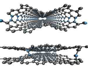 |
| ORNL simulations demonstrate how loops (seen above in blue) between graphene layers can be minimized using electron irradiation (bottom). |
Abstract:
Nanoscale simulations and theoretical research performed at the Department of Energy's Oak Ridge National Laboratory are bringing scientists closer to realizing graphene's potential in electronic applications.
ORNL scientists help explain graphene mystery
Oak Ridge, TN | Posted on August 24th, 2010A research team led by ORNL's Bobby Sumpter, Vincent Meunier and Eduardo Cruz-Silva has discovered how loops develop in graphene, an electrically conductive high-strength low-weight material that resembles an atomic-scale honeycomb.
Structural loops that sometimes form during a graphene cleaning process can render the material unsuitable for electronic applications. Overcoming these types of problems is of great interest to the electronics industry.
"Graphene is a rising star in the materials world, given its potential for use in precise electronic components like transistors or other semiconductors," said Bobby Sumpter, a staff scientist at ORNL.
The team used quantum molecular dynamics to simulate an experimental graphene cleaning process, as discussed in a paper published in Physical Review Letters. Calculations performed on ORNL supercomputers pointed the researchers to an overlooked intermediate step during processing.
Imaging with a transmission electron microscope, or TEM, subjected the graphene to electron irradiation, which ultimately prevented loop formation. The ORNL simulations showed that by injecting electrons to collect an image, the electrons were simultaneously changing the material's structure.
"Taking a picture with a TEM is not merely taking a picture," Sumpter said. "You might modify the picture at the same time that you're looking at it."
The research builds on findings discussed in a 2009 Science paper (Jia et al.), where Meunier and Sumpter helped demonstrate a process that cleans graphene edges by running a current through the material in a process known as Joule heating. Graphene is only as good as the uniformity or cleanliness of its edges, which determine how effectively the material can transmit electrons. Meunier said the ability to efficiently clean graphene edges is crucial to using the material in electronics.
"Imagine you have a fancy sports car, but then you realize it has square wheels. What good is it? That's like having jagged edges on graphene," Meunier said.
Recent experimental studies have shown that the Joule heating process can lead to undesirable loops that connect different graphene layers. The PRL paper provides an atomistic understanding of how electron irradiation from a transmission electron microscope affects the graphene cleaning process by preventing loop formation.
"We can clean the edges, and not only that, we're able to understand why we can clean them," Meunier said.
The research team included scientists from Massachusetts Institute of Technology, Universite Catholique de Louvain and Carlos III University of Madrid. Sumpter and Meunier are members of ORNL's Computer Science and Mathematics division with appointments in the Nanomaterials Theory Institute within the Center for Nanophase Materials Sciences. Cruz-Silva is a post-doctoral researcher at ORNL.
Part of this work was supported by the Center for Nanophase Materials Sciences (CNMS) at ORNL. CNMS is one of the five DOE Nanoscale Science Research Centers supported by the DOE Office of Science, premier national user facilities for interdisciplinary research at the nanoscale. Together the NSRCs comprise a suite of complementary facilities that provide researchers with state-of-the-art capabilities to fabricate, process, characterize and model nanoscale materials, and constitute the largest infrastructure investment of the National Nanotechnology Initiative. The NSRCs are located at DOE's Argonne, Brookhaven, Lawrence Berkeley, Oak Ridge and Sandia and Los Alamos national laboratories. For more information about the DOE NSRCs, please visit nano.energy.gov. ORNL is managed by UT-Battelle for the Department of Energy's Office of Science.
####
For more information, please click here
Copyright © Oak Ridge National Laboratory
If you have a comment, please Contact us.Issuers of news releases, not 7th Wave, Inc. or Nanotechnology Now, are solely responsible for the accuracy of the content.
Bookmark:


| Related News Press |
News and information
![]() Quantum computer improves AI predictions April 17th, 2026
Quantum computer improves AI predictions April 17th, 2026
![]() Flexible sensor gains sensitivity under pressure April 17th, 2026
Flexible sensor gains sensitivity under pressure April 17th, 2026
![]() A reusable chip for particulate matter sensing April 17th, 2026
A reusable chip for particulate matter sensing April 17th, 2026
![]() Detecting vibrational quantum beating in the predissociation dynamics of SF6 using time-resolved photoelectron spectroscopy April 17th, 2026
Detecting vibrational quantum beating in the predissociation dynamics of SF6 using time-resolved photoelectron spectroscopy April 17th, 2026
Govt.-Legislation/Regulation/Funding/Policy
![]() Quantum computer improves AI predictions April 17th, 2026
Quantum computer improves AI predictions April 17th, 2026
![]() Metasurfaces smooth light to boost magnetic sensing precision January 30th, 2026
Metasurfaces smooth light to boost magnetic sensing precision January 30th, 2026
![]() New imaging approach transforms study of bacterial biofilms August 8th, 2025
New imaging approach transforms study of bacterial biofilms August 8th, 2025
Possible Futures
![]() A fundamentally new therapeutic approach to cystic fibrosis: Nanobody repairs cellular defect April 17th, 2026
A fundamentally new therapeutic approach to cystic fibrosis: Nanobody repairs cellular defect April 17th, 2026
![]() UC Irvine physicists discover method to reverse �quantum scrambling� : The work addresses the problem of information loss in quantum computing system April 17th, 2026
UC Irvine physicists discover method to reverse �quantum scrambling� : The work addresses the problem of information loss in quantum computing system April 17th, 2026
Nanotubes/Buckyballs/Fullerenes/Nanorods/Nanostrings/Nanosheets
![]() Tiny nanosheets, big leap: A new sensor detects ethanol at ultra-low levels January 30th, 2026
Tiny nanosheets, big leap: A new sensor detects ethanol at ultra-low levels January 30th, 2026
![]() Enhancing power factor of p- and n-type single-walled carbon nanotubes April 25th, 2025
Enhancing power factor of p- and n-type single-walled carbon nanotubes April 25th, 2025
![]() Chainmail-like material could be the future of armor: First 2D mechanically interlocked polymer exhibits exceptional flexibility and strength January 17th, 2025
Chainmail-like material could be the future of armor: First 2D mechanically interlocked polymer exhibits exceptional flexibility and strength January 17th, 2025
![]() Innovative biomimetic superhydrophobic coating combines repair and buffering properties for superior anti-erosion December 13th, 2024
Innovative biomimetic superhydrophobic coating combines repair and buffering properties for superior anti-erosion December 13th, 2024
Announcements
![]() A fundamentally new therapeutic approach to cystic fibrosis: Nanobody repairs cellular defect April 17th, 2026
A fundamentally new therapeutic approach to cystic fibrosis: Nanobody repairs cellular defect April 17th, 2026
![]() UC Irvine physicists discover method to reverse �quantum scrambling� : The work addresses the problem of information loss in quantum computing system April 17th, 2026
UC Irvine physicists discover method to reverse �quantum scrambling� : The work addresses the problem of information loss in quantum computing system April 17th, 2026
Research partnerships
![]() Lab to industry: InSe wafer-scale breakthrough for future electronics August 8th, 2025
Lab to industry: InSe wafer-scale breakthrough for future electronics August 8th, 2025
![]() HKU physicists uncover hidden order in the quantum world through deconfined quantum critical points April 25th, 2025
HKU physicists uncover hidden order in the quantum world through deconfined quantum critical points April 25th, 2025
|
|
||
|
|
||
| The latest news from around the world, FREE | ||
|
|
||
|
|
||
| Premium Products | ||
|
|
||
|
Only the news you want to read!
Learn More |
||
|
|
||
|
Full-service, expert consulting
Learn More |
||
|
|
||