Home > Press > Fractals make better superconductors
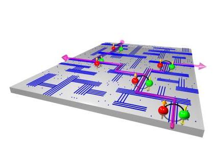 |
| Heat treatment improves the superconductivity of a ceramic copper oxide by creating a fractal network of connected channels of ordered oxygen defects. The green and red spheres represent the paired electrons responsible for superconductivity. Artwork by Manuel Vogtli (LCN). |
Abstract:
A team from Rome, Grenoble and London report that the strength of the superconductivity - its ability to persist as temperature is increased- correlates in certain oxide materials with structures visible over a range of length scales. I
Fractals make better superconductors
UK | Posted on August 12th, 2010Superconductivity, where a material conducts electricity at very low temperature with no resistance, and therefore transmission wastes virtually no energy, has applications ranging from medical scanners to maglev trains. Until now, scientists have focused on atomic-scale phenomena to explain this mysterious property of some special compounds. But in this week's Nature, a team from Rome, Grenoble and London report that the strength of the superconductivity - its ability to persist as temperature is increased- correlates in certain oxide materials with structures visible over a range of length scales. Intriguingly, these structures extend almost to the millimeter scale, and have a "fractal" nature, similar to the intricate patterns in a snowflake.
Since the discovery of superconductivity at the beginning of the last century, there has been a constant quest for improved performance in the form of higher operating temperatures and capacity to carry electrical power. A major breakthrough occurred in 1987 when two scientists from IBM discovered that oxides of copper, previously thought to be most unlikely candidates for superconductivity, superconduct at unprecedentedly high temperatures. Since then, this class of materials continues to hold the record for operating temperatures, well above the boiling temperature of inexpensive liquid nitrogen. At the same time, though, there is no agreement as to the mechanism underlying this high performance, even though a clear understanding would be extremely beneficial for engineers.
Until now, scientists have focused on structure at the nanometer (0.0000001 millimeters) - the distance between neighbouring atoms - scale as the determinant of the unusually strong superconductivity of the oxides of copper. For this week's Nature article, the researchers used the new technique of X-ray microscopy to examine a copper oxide superconductor whose internal structure could be changed via simple heat treatments - an approach employed by ceramicists over millennia to modify oxide materials.
The team discovered that the best superconductivity was obtained when the microstructure was most �connected', meaning that it is possible to trace a path with the same nanostructure (exhibited by oxygen atoms) over a large distance. The microstructure in this case was �fractal': if we were to zoom in on the material's structure at increasing levels of magnification, its appearance would remain the same.
Co-author Antonio Bianconi of the University Rome noted that "We are very excited by our results because they show that fractals, which are ubiquitous in both the biological sciences and the social sciences where they are even used to contemplate the behaviour of financial markets, now appear to have a significant impact on a fundamental property of inorganic matter, its superconductivity. " Co-author Gabriel Aeppli of the London Centre for Nanotechnology and University College London, added that "While there is no detailed theoretical explanation for what we have discovered yet, it demonstrates that classical ceramic engineering - with visible effects at near millimeter scales - can collude with quantum physics to produce the best superconductors."
The article is published in Nature (doi:10.1038/nature09260) on 12 Aug 2010. Click here (*) to see the article and associated News and Views on Nature's website
(*) www.nature.com/nature/journal/v466/n7308/full/nature09260.html
####
About London Centre for Nanotechnology
The London Centre for Nanotechnology is an interdisciplinary joint enterprise between University College London and Imperial College London. In bringing together world-class infrastructure and leading nanotechnology research activities, the Centre has the critical mass to compete with the best facilities world-wide. Research programmes are aligned to three key areas, namely Planet Care, Healthcare and Information Technology and exploit core competencies in the biomedical, physical and engineering sciences. Website: www.london-nano.com
For more information, please click here
Contacts:
UCL Press Office
David Weston
tel. +44-20 7679 7678
Copyright © London Centre for Nanotechnology
If you have a comment, please Contact us.Issuers of news releases, not 7th Wave, Inc. or Nanotechnology Now, are solely responsible for the accuracy of the content.
Bookmark:


| Related News Press |
News and information
![]() Quantum computer improves AI predictions April 17th, 2026
Quantum computer improves AI predictions April 17th, 2026
![]() Flexible sensor gains sensitivity under pressure April 17th, 2026
Flexible sensor gains sensitivity under pressure April 17th, 2026
![]() A reusable chip for particulate matter sensing April 17th, 2026
A reusable chip for particulate matter sensing April 17th, 2026
![]() Detecting vibrational quantum beating in the predissociation dynamics of SF6 using time-resolved photoelectron spectroscopy April 17th, 2026
Detecting vibrational quantum beating in the predissociation dynamics of SF6 using time-resolved photoelectron spectroscopy April 17th, 2026
Possible Futures
![]() A fundamentally new therapeutic approach to cystic fibrosis: Nanobody repairs cellular defect April 17th, 2026
A fundamentally new therapeutic approach to cystic fibrosis: Nanobody repairs cellular defect April 17th, 2026
![]() UC Irvine physicists discover method to reverse �quantum scrambling� : The work addresses the problem of information loss in quantum computing system April 17th, 2026
UC Irvine physicists discover method to reverse �quantum scrambling� : The work addresses the problem of information loss in quantum computing system April 17th, 2026
Academic/Education
![]() Rice University launches Rice Synthetic Biology Institute to improve lives January 12th, 2024
Rice University launches Rice Synthetic Biology Institute to improve lives January 12th, 2024
![]() Multi-institution, $4.6 million NSF grant to fund nanotechnology training September 9th, 2022
Multi-institution, $4.6 million NSF grant to fund nanotechnology training September 9th, 2022
Discoveries
![]() Quantum computer improves AI predictions April 17th, 2026
Quantum computer improves AI predictions April 17th, 2026
![]() Flexible sensor gains sensitivity under pressure April 17th, 2026
Flexible sensor gains sensitivity under pressure April 17th, 2026
![]() A reusable chip for particulate matter sensing April 17th, 2026
A reusable chip for particulate matter sensing April 17th, 2026
![]() Detecting vibrational quantum beating in the predissociation dynamics of SF6 using time-resolved photoelectron spectroscopy April 17th, 2026
Detecting vibrational quantum beating in the predissociation dynamics of SF6 using time-resolved photoelectron spectroscopy April 17th, 2026
Announcements
![]() A fundamentally new therapeutic approach to cystic fibrosis: Nanobody repairs cellular defect April 17th, 2026
A fundamentally new therapeutic approach to cystic fibrosis: Nanobody repairs cellular defect April 17th, 2026
![]() UC Irvine physicists discover method to reverse �quantum scrambling� : The work addresses the problem of information loss in quantum computing system April 17th, 2026
UC Irvine physicists discover method to reverse �quantum scrambling� : The work addresses the problem of information loss in quantum computing system April 17th, 2026
Research partnerships
![]() Lab to industry: InSe wafer-scale breakthrough for future electronics August 8th, 2025
Lab to industry: InSe wafer-scale breakthrough for future electronics August 8th, 2025
![]() HKU physicists uncover hidden order in the quantum world through deconfined quantum critical points April 25th, 2025
HKU physicists uncover hidden order in the quantum world through deconfined quantum critical points April 25th, 2025
Quantum nanoscience
![]() Beyond silicon: Electronics at the scale of a single molecule January 30th, 2026
Beyond silicon: Electronics at the scale of a single molecule January 30th, 2026
![]() MXene nanomaterials enter a new dimension Multilayer nanomaterial: MXene flakes created at Drexel University show new promise as 1D scrolls January 30th, 2026
MXene nanomaterials enter a new dimension Multilayer nanomaterial: MXene flakes created at Drexel University show new promise as 1D scrolls January 30th, 2026
![]() ICFO researchers overcome long-standing bottleneck in single photon detection with twisted 2D materials August 8th, 2025
ICFO researchers overcome long-standing bottleneck in single photon detection with twisted 2D materials August 8th, 2025
|
|
||
|
|
||
| The latest news from around the world, FREE | ||
|
|
||
|
|
||
| Premium Products | ||
|
|
||
|
Only the news you want to read!
Learn More |
||
|
|
||
|
Full-service, expert consulting
Learn More |
||
|
|
||