Home > Press > Researchers demonstrate highly directional terahertz laser rays
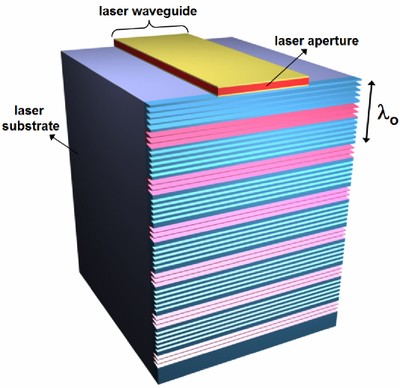 |
| Schematic diagram of a terahertz quantum cascade laser patterned with a metamaterial collimator. The metamaterial patterns are directly sculpted on the highly doped GaAs facet of the device. Artificial coloring in the figure indicates deep and shallow micron scale grooves, which have different functions. The shallow �blue� grooves efficiently couple laser output into surface electromagnetic waves on the facet and confine the waves to the facet. The deep �pink� grooves form an effective grating that coherently scatters the energy of the surface waves into the far-field. |
Abstract:
Advance in metamaterials leads to a new semiconductor laser suitable for security screening, chemical sensing and astronomy
Researchers demonstrate highly directional terahertz laser rays
Cambridge, MA & Leeds, UK | Posted on August 10th, 2010A collaborative team of applied scientists from Harvard University and the University of Leeds have demonstrated a new terahertz (THz) semiconductor laser that emits beams with a much smaller divergence than conventional THz laser sources. The advance, published in the August 8th issue of Nature Materials, opens the door to a wide range of applications in terahertz science and technology. Harvard has filed a broad patent on the invention.
The finding was spearheaded by postdoctoral fellow Nanfang Yu and Federico Capasso, Robert L. Wallace Professor of Applied Physics and Vinton Hayes Senior Research Fellow in Electrical Engineering, both of Harvard's School of Engineering and Applied Sciences (SEAS), and by a team led by Edmund Linfield at the School of Electronic and Electrical Engineering, University of Leeds.
Terahertz rays (T-rays) can penetrate efficiently through paper, clothing, plastic, and many other materials, making them ideal for detecting concealed weapons and biological agents, imaging tumors without harmful side effects, and spotting defects, such as cracks, within materials. THz radiation is also used for high-sensitivity detection of tiny concentrations of interstellar chemicals.
"Unfortunately, present THz semiconductor lasers are not suitable for many of these applications because their beam is widely divergent�similar to how light is emitted from a lamp" says Capasso. "By creating an artificial optical structure on the facet of the laser, we were able to generate highly collimated (i.e., tightly bound) rays from the device. This leads to the efficient collection and high concentration of power without the need for conventional, expensive, and bulky lenses."
Specifically, to get around the conventional limitations, the researchers sculpted an array of sub-wavelength-wide grooves, dubbed a metamaterial, directly on the facet of quantum cascade lasers. The devices emit at a frequency of 3 THz (or a wavelength of one hundred microns), in the invisible part of the spectrum known as the far-infrared.
"Our team was able to reduce the divergence angle of the beam emerging from these semiconductor lasers dramatically, whilst maintaining the high output optical power of identical unpatterned devices," says Linfield. "This type of laser could be used by customs officials to detect illicit substances and by pharmaceutical manufacturers to check the quality of drugs being produced and stored."
The use of metamaterials, artificial materials engineered to provide properties which may not be readily available in Nature, was critical to the researchers' successful demonstration. While metamaterials have potential use in novel applications such as cloaking, negative refraction and high resolution imaging, their use in semiconductor devices has been very limited to date.
"In our case, the metamaterial serves a dual function: strongly confining the THz light emerging from the device to the laser facet and collimating the beam," explains Yu. "The ability of metamaterials to confine strongly THz waves to surfaces makes it possible to manipulate them efficiently for applications such as sensing and THz optical circuits."
Additional co-authors of the study included Qi Jie Wang, formerly of Harvard University and now with the Nanyang Technological University in Singapore; graduate student Mikhail A. Kats and postdoctoral fellow Jonathan A. Fan, both of Harvard University; and postdoctoral fellows Suraj P. Khanna and Lianhe Li and faculty member A. Giles Davies, all from the University of Leeds.
The research was partially supported by the Air Force Office of Scientific Research. The Harvard-based authors also acknowledge the support of the Center for Nanoscale Systems (CNS) at Harvard University, a member of the National Nanotechnology Infrastructure Network (NNIN). The Leeds-based authors acknowledge support from the UK's Engineering and Physical Sciences Research Council.
Quantum Cascade Lasers were first invented and demonstrated by Federico Capasso and his team at Bell Labs in 1994. At the shorter wavelengths of the mid-infrared spectrum these compact millimeter length semiconductor lasers operate routinely at room temperature with high optical powers and are a rapidly growing commercial sector for a wide range of military and civilian applications including infrared countermeasures and chemical sensing. They are made by stacking ultra-thin atomic layers of semiconductor materials on top of each other. By varying the thickness of the layers one can design the energy levels in the structure to create an artificial laser medium.
####
For more information, please click here
Copyright © Harvard University
If you have a comment, please Contact us.Issuers of news releases, not 7th Wave, Inc. or Nanotechnology Now, are solely responsible for the accuracy of the content.
Bookmark:


| Related News Press |
News and information
![]() Quantum computer improves AI predictions April 17th, 2026
Quantum computer improves AI predictions April 17th, 2026
![]() Flexible sensor gains sensitivity under pressure April 17th, 2026
Flexible sensor gains sensitivity under pressure April 17th, 2026
![]() A reusable chip for particulate matter sensing April 17th, 2026
A reusable chip for particulate matter sensing April 17th, 2026
![]() Detecting vibrational quantum beating in the predissociation dynamics of SF6 using time-resolved photoelectron spectroscopy April 17th, 2026
Detecting vibrational quantum beating in the predissociation dynamics of SF6 using time-resolved photoelectron spectroscopy April 17th, 2026
Govt.-Legislation/Regulation/Funding/Policy
![]() Quantum computer improves AI predictions April 17th, 2026
Quantum computer improves AI predictions April 17th, 2026
![]() Metasurfaces smooth light to boost magnetic sensing precision January 30th, 2026
Metasurfaces smooth light to boost magnetic sensing precision January 30th, 2026
![]() New imaging approach transforms study of bacterial biofilms August 8th, 2025
New imaging approach transforms study of bacterial biofilms August 8th, 2025
Possible Futures
![]() A fundamentally new therapeutic approach to cystic fibrosis: Nanobody repairs cellular defect April 17th, 2026
A fundamentally new therapeutic approach to cystic fibrosis: Nanobody repairs cellular defect April 17th, 2026
![]() UC Irvine physicists discover method to reverse �quantum scrambling� : The work addresses the problem of information loss in quantum computing system April 17th, 2026
UC Irvine physicists discover method to reverse �quantum scrambling� : The work addresses the problem of information loss in quantum computing system April 17th, 2026
Academic/Education
![]() Rice University launches Rice Synthetic Biology Institute to improve lives January 12th, 2024
Rice University launches Rice Synthetic Biology Institute to improve lives January 12th, 2024
![]() Multi-institution, $4.6 million NSF grant to fund nanotechnology training September 9th, 2022
Multi-institution, $4.6 million NSF grant to fund nanotechnology training September 9th, 2022
Announcements
![]() A fundamentally new therapeutic approach to cystic fibrosis: Nanobody repairs cellular defect April 17th, 2026
A fundamentally new therapeutic approach to cystic fibrosis: Nanobody repairs cellular defect April 17th, 2026
![]() UC Irvine physicists discover method to reverse �quantum scrambling� : The work addresses the problem of information loss in quantum computing system April 17th, 2026
UC Irvine physicists discover method to reverse �quantum scrambling� : The work addresses the problem of information loss in quantum computing system April 17th, 2026
Photonics/Optics/Lasers
![]() Metasurfaces smooth light to boost magnetic sensing precision January 30th, 2026
Metasurfaces smooth light to boost magnetic sensing precision January 30th, 2026
![]() From sensors to smart systems: the rise of AI-driven photonic noses January 30th, 2026
From sensors to smart systems: the rise of AI-driven photonic noses January 30th, 2026
Research partnerships
![]() Lab to industry: InSe wafer-scale breakthrough for future electronics August 8th, 2025
Lab to industry: InSe wafer-scale breakthrough for future electronics August 8th, 2025
![]() HKU physicists uncover hidden order in the quantum world through deconfined quantum critical points April 25th, 2025
HKU physicists uncover hidden order in the quantum world through deconfined quantum critical points April 25th, 2025
Quantum nanoscience
![]() Beyond silicon: Electronics at the scale of a single molecule January 30th, 2026
Beyond silicon: Electronics at the scale of a single molecule January 30th, 2026
![]() MXene nanomaterials enter a new dimension Multilayer nanomaterial: MXene flakes created at Drexel University show new promise as 1D scrolls January 30th, 2026
MXene nanomaterials enter a new dimension Multilayer nanomaterial: MXene flakes created at Drexel University show new promise as 1D scrolls January 30th, 2026
![]() ICFO researchers overcome long-standing bottleneck in single photon detection with twisted 2D materials August 8th, 2025
ICFO researchers overcome long-standing bottleneck in single photon detection with twisted 2D materials August 8th, 2025
|
|
||
|
|
||
| The latest news from around the world, FREE | ||
|
|
||
|
|
||
| Premium Products | ||
|
|
||
|
Only the news you want to read!
Learn More |
||
|
|
||
|
Full-service, expert consulting
Learn More |
||
|
|
||