Home > Press > Scientists Create Nano-Patterned Superconducting Thin Films
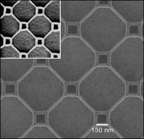 |
| A fragment of a superconducting thin film patterned with nano-loops measuring 150 nanometers on a side (small) and 500 nanometers on a side (large), where the nano wires making up each loop have a diameter of 25 nanometers. |
Abstract:
Material's fluctuating response to a magnetic field could lead to switchable superconducting wires
Scientists Create Nano-Patterned Superconducting Thin Films
Upton, NY | Posted on June 14th, 2010A team of scientists from Bar-Ilan University, Israel, and the U.S. Department of Energy's (DOE) Brookhaven National Laboratory has fabricated thin films patterned with large arrays of nanowires and loops that are superconducting � able to carry electric current with no resistance � when cooled below about 30 kelvin (-243 degrees Celsius). Even more interesting, the scientists showed they could change the material's electrical resistance in an unexpected way by placing the material in an external magnetic field.
"Such superconducting nanowires and nano-loops might eventually be useful for new electronic devices � that is the long-term vision," said Brookhaven Lab physicist Ivan Bozovic, who synthesized the superconducting films. "That is the long-term vision."
He and his collaborators describe the research in Nature Nanotechnology, published online June 13, 2010.
It has been a long-standing dream to fabricate superconducting nano-scale wires for faster, more powerful electronics. However, this has turned out to be very difficult if not impossible with conventional superconductors because the minimal size for the sample to be superconducting � known as the coherence length � is large. For example, in the case of niobium, the most widely used superconductor, it is about 40 nanometers. Very thin nano-wires made of such materials wouldn't act as superconductors.
However, in layered copper-oxide superconductors, the coherence length is much smaller � about one or two nanometers within the copper-oxide plane, and as small as a tenth of a nanometer out-of-plane. The fact that these materials operate at warmer temperatures, reducing the need for costly cooling, makes them even more attractive for real-world applications.
To see if they could achieve superconductivity in a thin film material etched to form a pattern of "wires" � much like the circuits etched into computer chips � the Brookhaven team started by using a precision technique for making superconducting thin films atomic layer by layer. They used molecular beam epitaxy to build a material with alternating layers of copper-oxide and lanthanum and strontium. Bozovic's team had previously used this technique to produce thin films that retain superconductivity within a single copper-oxide layer.
Then the team at Bar-Ilan used electron-beam lithography to "etch" a pattern of thousands of loops into the surface of the material. The thickness, or diameter, of the "nanowires" forming the sides of these loops was mere 25 nanometers, while the lengths ranged from 150 to 500 nanometers. Measurements of electrical resistance of the patterned arrays showed that they were indeed superconducting when cooled below about 30 K.
When the scientists applied an external magnetic field perpendicular to the loops, they found that the loop resistance did not keep increasing steadily with the field strength, but rather changed up and down in an oscillatory manner.
"These oscillations in resistance have a large amplitude, and their frequency corresponds to discrete units (quanta) of magnetic flux � the measure of the strength of the magnetic field piercing the loops," Bozovic said. "A material with such a discrete, switchable form of magneto-resistance � especially from the superconducting to the non-superconducting state � could be extremely useful for engineering new devices."
The observed frequency of the oscillations in resistance may also have implications for understanding the mechanism by which copper-oxide materials become superconductors in the first place. The current findings seem to rule out certain theoretical models that propose that an ordered alignment of charge carriers known as "stripes" is essential to superconductivity in copper-oxide compounds. A better understanding of the mechanism of superconductivity could lead to even more advances in designing new materials for practical applications.
The Brookhaven scientists' role in this research was supported by DOE's Office of Science. The work was also funded by the German Research Foundation through a German-Israeli cooperative agreement, and by a scholarship granted by the Israel Ministry of Science.
####
About Brookhaven National Laboratory
One of ten national laboratories overseen and primarily funded by the Office of Science of the U.S. Department of Energy (DOE), Brookhaven National Laboratory conducts research in the physical, biomedical, and environmental sciences, as well as in energy technologies and national security. Brookhaven Lab also builds and operates major scientific facilities available to university, industry and government researchers. Brookhaven is operated and managed for DOE's Office of Science by Brookhaven Science Associates, a limited-liability company founded by Stony Brook University, the largest academic user of Laboratory facilities, and Battelle, a nonprofit, applied science and technology organization.
For more information, please click here
Contacts:
Karen McNulty Walsh
(631)344-8350
Peter Genzer
(631) 344-3174
Copyright © Brookhaven National Laboratory
If you have a comment, please Contact us.Issuers of news releases, not 7th Wave, Inc. or Nanotechnology Now, are solely responsible for the accuracy of the content.
Bookmark:


| Related News Press |
News and information
![]() Simulating magnetization in a Heisenberg quantum spin chain April 5th, 2024
Simulating magnetization in a Heisenberg quantum spin chain April 5th, 2024
![]() NRL charters Navy�s quantum inertial navigation path to reduce drift April 5th, 2024
NRL charters Navy�s quantum inertial navigation path to reduce drift April 5th, 2024
![]() Discovery points path to flash-like memory for storing qubits: Rice find could hasten development of nonvolatile quantum memory April 5th, 2024
Discovery points path to flash-like memory for storing qubits: Rice find could hasten development of nonvolatile quantum memory April 5th, 2024
![]() Good as gold - improving infectious disease testing with gold nanoparticles April 5th, 2024
Good as gold - improving infectious disease testing with gold nanoparticles April 5th, 2024
Thin films
![]() Utilizing palladium for addressing contact issues of buried oxide thin film transistors April 5th, 2024
Utilizing palladium for addressing contact issues of buried oxide thin film transistors April 5th, 2024
![]() Understanding the mechanism of non-uniform formation of diamond film on tools: Paving the way to a dry process with less environmental impact March 24th, 2023
Understanding the mechanism of non-uniform formation of diamond film on tools: Paving the way to a dry process with less environmental impact March 24th, 2023
![]() New study introduces the best graphite films: The work by Distinguished Professor Feng Ding at UNIST has been published in the October 2022 issue of Nature Nanotechnology November 4th, 2022
New study introduces the best graphite films: The work by Distinguished Professor Feng Ding at UNIST has been published in the October 2022 issue of Nature Nanotechnology November 4th, 2022
Govt.-Legislation/Regulation/Funding/Policy
![]() NRL charters Navy�s quantum inertial navigation path to reduce drift April 5th, 2024
NRL charters Navy�s quantum inertial navigation path to reduce drift April 5th, 2024
![]() Discovery points path to flash-like memory for storing qubits: Rice find could hasten development of nonvolatile quantum memory April 5th, 2024
Discovery points path to flash-like memory for storing qubits: Rice find could hasten development of nonvolatile quantum memory April 5th, 2024
![]() Chemical reactions can scramble quantum information as well as black holes April 5th, 2024
Chemical reactions can scramble quantum information as well as black holes April 5th, 2024
Possible Futures
![]() Discovery points path to flash-like memory for storing qubits: Rice find could hasten development of nonvolatile quantum memory April 5th, 2024
Discovery points path to flash-like memory for storing qubits: Rice find could hasten development of nonvolatile quantum memory April 5th, 2024
![]() With VECSELs towards the quantum internet Fraunhofer: IAF achieves record output power with VECSEL for quantum frequency converters April 5th, 2024
With VECSELs towards the quantum internet Fraunhofer: IAF achieves record output power with VECSEL for quantum frequency converters April 5th, 2024
Academic/Education
![]() Rice University launches Rice Synthetic Biology Institute to improve lives January 12th, 2024
Rice University launches Rice Synthetic Biology Institute to improve lives January 12th, 2024
![]() Multi-institution, $4.6 million NSF grant to fund nanotechnology training September 9th, 2022
Multi-institution, $4.6 million NSF grant to fund nanotechnology training September 9th, 2022
Announcements
![]() NRL charters Navy�s quantum inertial navigation path to reduce drift April 5th, 2024
NRL charters Navy�s quantum inertial navigation path to reduce drift April 5th, 2024
![]() Discovery points path to flash-like memory for storing qubits: Rice find could hasten development of nonvolatile quantum memory April 5th, 2024
Discovery points path to flash-like memory for storing qubits: Rice find could hasten development of nonvolatile quantum memory April 5th, 2024
Research partnerships
![]() Discovery points path to flash-like memory for storing qubits: Rice find could hasten development of nonvolatile quantum memory April 5th, 2024
Discovery points path to flash-like memory for storing qubits: Rice find could hasten development of nonvolatile quantum memory April 5th, 2024
![]() Researchers� approach may protect quantum computers from attacks March 8th, 2024
Researchers� approach may protect quantum computers from attacks March 8th, 2024
![]() 'Sudden death' of quantum fluctuations defies current theories of superconductivity: Study challenges the conventional wisdom of superconducting quantum transitions January 12th, 2024
'Sudden death' of quantum fluctuations defies current theories of superconductivity: Study challenges the conventional wisdom of superconducting quantum transitions January 12th, 2024
|
|
||
|
|
||
| The latest news from around the world, FREE | ||
|
|
||
|
|
||
| Premium Products | ||
|
|
||
|
Only the news you want to read!
Learn More |
||
|
|
||
|
Full-service, expert consulting
Learn More |
||
|
|
||