Home > Press > Ferroelectrics: Useful imperfections
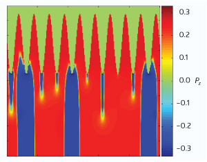 |
| Fig. 1: Simulation results showing the electric polarization in a cross-section of a nanoscale ferroelectric thin film with a periodically modulated surface. The inhomogeneous electric field distribution, caused by the non-flat surface, gives rise to nucleation sites where the electric polarization (Pz) is reversed (blue regions), These sites �spread� throughout the film as the absolute value of the applied electric field increases, until the polarity of the whole film is reversed. Reproduced from Ref. 1 � 2010 Institute of Physics and IOP Publishing |
Abstract:
Nanoscale surface variations of ferroelectric films may be harnessed for the design of future memory applications
Ferroelectrics: Useful imperfections
Singapore | Posted on February 3rd, 2010Ferroelectric thin films have the potential to become the building blocks for electronic memory applications but, as film thicknesses decrease with further miniaturization, surface imperfections can influence device performance. Rajeev Ahluwalia and co-workers at the Institute of High Performance Computing of A*STAR, Singapore, have now shown that even nanoscale modulations of the surface geometry can significantly influence a ferroelectric film's response to an applied electric field, yielding valuable information for the efficient design of nanotechnological devices based on such materials1.
Information in portable electronics is typically stored in semiconductor memories, where the information is encoded via the presence or absence of electric charges in transistor-based memory cells. In ferroelectrics, however, information is encoded in the orientation of electric dipoles formed in the material. This orientation is also known as the sign of the electric polarization and can be controlled by an externally applied electric field. According to Ahluwalia, the semiconductor industry's interest in ferroelectrics for memory applications lies in their prospective fast-operating characteristics as well as their ability to retain data even when powered off.
Ahluwalia and co-workers' theoretical study shows that even small deviations from a perfectly flat surface in a ferroelectric thin film may dramatically change the way its polarization switches sign in an applied electric field (Fig. 1). "The non-planar surface introduces nucleation sites due to an inhomogeneous electric field distribution," says Ahluwalia. These nucleation sites serve as �seeds' for the formation of domains of reversed polarization that grow with the increase of the absolute value of the electric field until the overall polarization of the film switches sign around the so-called coercive field.
The details of the dynamical evolution, or the �spreading', of the domains of reversed polarization, as well as the magnitude of the coercive field, are sensitive to the amplitude and length scale of the surface irregularities. "The surface effect will start playing a role when the amplitude of the roughness starts being comparable to the film thickness," explains Ahluwalia, which is consistent with the numerical results showing a decrease in the coercive field with increasing amplitude in roughness.
Despite the study being performed for material parameters corresponding to barium titanate, Ahluwalia predicts that the qualitative results should apply to many ferroelectric materials. He notes, however, that in the present model the domain dynamics are calculated based on a uniaxial ferroelectric. Further studies based on three-dimensional models are thus required to obtain quantitative predictions for specific device design.
The A*STAR affiliated authors in this highlight are from the Institute of High Performance Computing.
Reference
1. Ahluwalia, R., Ng, N. & Srolovitz, D.J. Surface morphology effects on polarization switching in nanoscale ferroelectrics. Nanotechnology 20, 445709 (2009).
####
About A*STAR
A*STAR Research is an online and print publication highlighting some of the best research and technological developments at the research institutes of Singapore�s Agency for Science, Technology and Research (A*STAR). Established in 2002, A*STAR has thrived as a global research organization with a principal mission of fostering world-class scientific research and talent for a vibrant knowledge-based Singapore. A*STAR currently oversees 14 research institutes as well as 7 consortia and centers located in the Biopolis and Fusionopolis complexes and the vicinity, and supports extramural research in collaboration with universities, hospital research centers and other local and international partners. The various A*STAR institutes are involved in research in a wide range of scientific fields, coordinated and funded by Singapore�s Biomedical Research Council (BMRC) and Science and Engineering Research Council (SERC).
For more information, please click here
Copyright © A*STAR
If you have a comment, please Contact us.Issuers of news releases, not 7th Wave, Inc. or Nanotechnology Now, are solely responsible for the accuracy of the content.
Bookmark:


| Related News Press |
News and information
![]() Simulating magnetization in a Heisenberg quantum spin chain April 5th, 2024
Simulating magnetization in a Heisenberg quantum spin chain April 5th, 2024
![]() NRL charters Navy�s quantum inertial navigation path to reduce drift April 5th, 2024
NRL charters Navy�s quantum inertial navigation path to reduce drift April 5th, 2024
![]() Discovery points path to flash-like memory for storing qubits: Rice find could hasten development of nonvolatile quantum memory April 5th, 2024
Discovery points path to flash-like memory for storing qubits: Rice find could hasten development of nonvolatile quantum memory April 5th, 2024
Possible Futures
![]() Discovery points path to flash-like memory for storing qubits: Rice find could hasten development of nonvolatile quantum memory April 5th, 2024
Discovery points path to flash-like memory for storing qubits: Rice find could hasten development of nonvolatile quantum memory April 5th, 2024
![]() With VECSELs towards the quantum internet Fraunhofer: IAF achieves record output power with VECSEL for quantum frequency converters April 5th, 2024
With VECSELs towards the quantum internet Fraunhofer: IAF achieves record output power with VECSEL for quantum frequency converters April 5th, 2024
Memory Technology
![]() Utilizing palladium for addressing contact issues of buried oxide thin film transistors April 5th, 2024
Utilizing palladium for addressing contact issues of buried oxide thin film transistors April 5th, 2024
![]() Interdisciplinary: Rice team tackles the future of semiconductors Multiferroics could be the key to ultralow-energy computing October 6th, 2023
Interdisciplinary: Rice team tackles the future of semiconductors Multiferroics could be the key to ultralow-energy computing October 6th, 2023
![]() Researchers discover materials exhibiting huge magnetoresistance June 9th, 2023
Researchers discover materials exhibiting huge magnetoresistance June 9th, 2023
Announcements
![]() NRL charters Navy�s quantum inertial navigation path to reduce drift April 5th, 2024
NRL charters Navy�s quantum inertial navigation path to reduce drift April 5th, 2024
![]() Discovery points path to flash-like memory for storing qubits: Rice find could hasten development of nonvolatile quantum memory April 5th, 2024
Discovery points path to flash-like memory for storing qubits: Rice find could hasten development of nonvolatile quantum memory April 5th, 2024
|
|
||
|
|
||
| The latest news from around the world, FREE | ||
|
|
||
|
|
||
| Premium Products | ||
|
|
||
|
Only the news you want to read!
Learn More |
||
|
|
||
|
Full-service, expert consulting
Learn More |
||
|
|
||