Home > Press > UAlbany NanoCollege and JSC Innovative Technopark in Republic of Tatarstan to Collaborate
 |
Abstract:
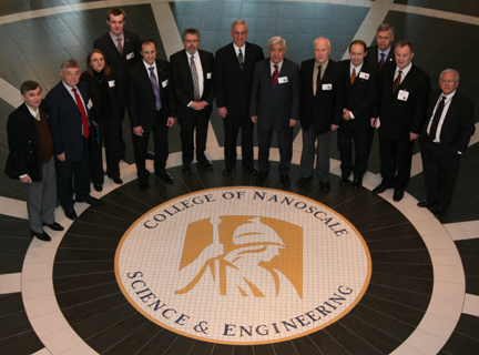
The College of Nanoscale Science and Engineering (CNSE) and the JSC Innovative Technopark (IDEA) in the Republic of Tatarstan today signed a Memorandum of Understanding to establish a framework for collaboration in nanotechnology education, research and commercialization.
UAlbany NanoCollege and JSC Innovative Technopark in Republic of Tatarstan to Collaborate
Albany, NY | Posted on January 28th, 2010Through the partnership, CNSE will provide assistance to, and participation with, IDEA in areas such as educational, research, and commercialization advisory functions, and consulting services to include specialized training courses for students, faculty and scientists of the Republic of Tatarstan at the CNSE facilities, and the potential creation and program design of nanotechnology centers both in Kazan and at CNSE.
In addition, the partnership provides opportunities for IDEA to procure research and development equipment, and to receive assistance in technology transfer and commercialization opportunities in critical nanotechnology-enabled industrial applications, such as green energy, health sciences and nanomedicine.
IDEA is one of the largest innovative technoparks in Europe, located in the city of Kazan, capital of the Republic of Tatarstan, with a mission to commercialize innovative ideas through the launch and development of small-sized companies through the activities of its three main subdivisions, including a business incubator, innovative technology center, and business park.
####
About CNSE
CNSE is the first college in the world dedicated to research, development, education, and deployment in the emerging disciplines of nanoscience, nanoengineering, nanobioscience, and nanoeconomics. With over $5 billion in public and private investments, CNSE's Albany NanoTech Complex -- the most advanced research complex at any university in the world - employs more than 2,500 scientists, researchers, engineers, faculty and students, and has attracted over 250 global corporate partners.
For more information, please click here
Contacts:
Press/Media Inquiries:
Steve Janack
CNSE Vice President for Marketing and Communications
Director of Communications Services
College of Nanoscale Science and Engineering
University at Albany
257 Fuller Road
Albany, NY 12203
Phone: 518-956-7322
Copyright © CNSE
If you have a comment, please Contact us.Issuers of news releases, not 7th Wave, Inc. or Nanotechnology Now, are solely responsible for the accuracy of the content.
Bookmark:


| Related News Press |
News and information
![]() Simulating magnetization in a Heisenberg quantum spin chain April 5th, 2024
Simulating magnetization in a Heisenberg quantum spin chain April 5th, 2024
![]() NRL charters Navy�s quantum inertial navigation path to reduce drift April 5th, 2024
NRL charters Navy�s quantum inertial navigation path to reduce drift April 5th, 2024
![]() Discovery points path to flash-like memory for storing qubits: Rice find could hasten development of nonvolatile quantum memory April 5th, 2024
Discovery points path to flash-like memory for storing qubits: Rice find could hasten development of nonvolatile quantum memory April 5th, 2024
Academic/Education
![]() Rice University launches Rice Synthetic Biology Institute to improve lives January 12th, 2024
Rice University launches Rice Synthetic Biology Institute to improve lives January 12th, 2024
![]() Multi-institution, $4.6 million NSF grant to fund nanotechnology training September 9th, 2022
Multi-institution, $4.6 million NSF grant to fund nanotechnology training September 9th, 2022
Nanomedicine
![]() New micromaterial releases nanoparticles that selectively destroy cancer cells April 5th, 2024
New micromaterial releases nanoparticles that selectively destroy cancer cells April 5th, 2024
![]() Good as gold - improving infectious disease testing with gold nanoparticles April 5th, 2024
Good as gold - improving infectious disease testing with gold nanoparticles April 5th, 2024
![]() Researchers develop artificial building blocks of life March 8th, 2024
Researchers develop artificial building blocks of life March 8th, 2024
Announcements
![]() NRL charters Navy�s quantum inertial navigation path to reduce drift April 5th, 2024
NRL charters Navy�s quantum inertial navigation path to reduce drift April 5th, 2024
![]() Discovery points path to flash-like memory for storing qubits: Rice find could hasten development of nonvolatile quantum memory April 5th, 2024
Discovery points path to flash-like memory for storing qubits: Rice find could hasten development of nonvolatile quantum memory April 5th, 2024
Patents/IP/Tech Transfer/Licensing
![]() Getting drugs across the blood-brain barrier using nanoparticles March 3rd, 2023
Getting drugs across the blood-brain barrier using nanoparticles March 3rd, 2023
![]() Metasurfaces control polarized light at will: New research unlocks the hidden potential of metasurfaces August 13th, 2021
Metasurfaces control polarized light at will: New research unlocks the hidden potential of metasurfaces August 13th, 2021
![]() Arrowhead Pharmaceuticals Announces Closing of Agreement with Takeda November 27th, 2020
Arrowhead Pharmaceuticals Announces Closing of Agreement with Takeda November 27th, 2020
Environment
![]() Billions of nanoplastics released when microwaving baby food containers: Exposure to plastic particles kills up to 75% of cultured kidney cells July 21st, 2023
Billions of nanoplastics released when microwaving baby food containers: Exposure to plastic particles kills up to 75% of cultured kidney cells July 21st, 2023
Energy
![]() Development of zinc oxide nanopagoda array photoelectrode: photoelectrochemical water-splitting hydrogen production January 12th, 2024
Development of zinc oxide nanopagoda array photoelectrode: photoelectrochemical water-splitting hydrogen production January 12th, 2024
![]() Shedding light on unique conduction mechanisms in a new type of perovskite oxide November 17th, 2023
Shedding light on unique conduction mechanisms in a new type of perovskite oxide November 17th, 2023
![]() Inverted perovskite solar cell breaks 25% efficiency record: Researchers improve cell efficiency using a combination of molecules to address different November 17th, 2023
Inverted perovskite solar cell breaks 25% efficiency record: Researchers improve cell efficiency using a combination of molecules to address different November 17th, 2023
![]() The efficient perovskite cells with a structured anti-reflective layer � another step towards commercialization on a wider scale October 6th, 2023
The efficient perovskite cells with a structured anti-reflective layer � another step towards commercialization on a wider scale October 6th, 2023
Alliances/Trade associations/Partnerships/Distributorships
![]() Chicago Quantum Exchange welcomes six new partners highlighting quantum technology solutions, from Chicago and beyond September 23rd, 2022
Chicago Quantum Exchange welcomes six new partners highlighting quantum technology solutions, from Chicago and beyond September 23rd, 2022
![]() University of Illinois Chicago joins Brookhaven Lab's Quantum Center June 10th, 2022
University of Illinois Chicago joins Brookhaven Lab's Quantum Center June 10th, 2022
|
|
||
|
|
||
| The latest news from around the world, FREE | ||
|
|
||
|
|
||
| Premium Products | ||
|
|
||
|
Only the news you want to read!
Learn More |
||
|
|
||
|
Full-service, expert consulting
Learn More |
||
|
|
||