Home > Press > Absorbing Hydrogen Fluoride Gas to Enhance Crystal Growth
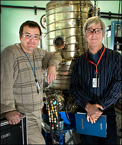 |
| Vyacheslav Solovyov (left) and Harold "Bud" Wiesmann |
Abstract:
Newly patented method could improve superconductors, optical devices, and microelectronics.
Absorbing Hydrogen Fluoride Gas to Enhance Crystal Growth
Upton, NY | Posted on December 10th, 2009Two scientists at the U.S. Department of Energy's (DOE) Brookhaven National Laboratory have developed a method to control the buildup of hydrogen fluoride gas during the growth of precision crystals needed for applications such as superconductors, optical devices, and microelectronics. The invention � by Vyacheslav Solovyov and Harold Wiesmann and recently awarded U.S. Patent number 7,622,426 � could lead to more efficient production and improved performance of these materials.
Materials with highly ordered crystalline atomic structures have enormous potential for energy-saving devices such as superconductors, which carry current with no energy loss, and high-speed electronics. Such crystals are typically grown from precursors deposited on substrates � for example: tapes, wires, or wafers, such as those used in the production of computer chips.
Adding fluorine to the precursors enhances the transfer of crystalline order from the substrate to the growing material. But fluorine also presents a problem because it leads to the buildup of hydrogen fluoride gas. Hydrogen fluoride slows down the reaction that converts the precursor to the desired material, sometimes even stopping crystal growth in its tracks.
"You might think you could just vent the accumulating gas, but such methods have proven impractical," said Wiesmann. For one thing, you'd have to remove the gas uniformly, to avoid variations in pressure that might affect crystal growth, which becomes more difficult over larger areas. Also, other gases necessary to crystal growth, such as oxygen and water vapor, get extracted along with the hydrogen fluoride, and re-injecting these gases introduces more pressure problems.
"We've developed an improved method for removing hydrogen fluoride, based on absorption, that enhances the production of high-quality crystalline products." Wiesmann said.
The new method incorporates a solid material capable of absorbing hydrogen fluoride (HF) gas inside the reaction chamber. The solid material can be attached to the inner surface of the reaction chamber or free standing, as long as it is made to conform to the shape of the precursor at a uniform distance. This allows uniform extraction of HF across large areas, thereby yielding crystalline end products that are uniform and homogeneous regardless of the shape of the precursor material or the area it occupies inside the reaction chamber.
A wide range of materials from alkaline earth oxides to materials containing calcium, sodium, or even activated carbon can be used as HF absorbers. The HF absorber material could be sprayed, painted, or otherwise deposited onto an inert support such as quartz or various oxides to attach it to the reaction chamber. Or it could be made from a powder and pressed into a form that conforms to the shape of the growing crystals.
"Because these materials selectively absorb HF gas, water vapor, oxygen, and other gases that may be present and necessary for the conversion of the precursor material to finished crystals remain in the reaction vessel, undisturbed," Solovyov said.
Solovyov and Wiesmann demonstrated the effectiveness of this approach when growing crystals of a common yttrium-barium-copper-oxide (YBCO) superconductor. In these experiments, YBCO crystals grew at a faster rate in the presence of a barium-oxide HF absorber when compared to conventional methods of crystal growth. The method also preserves the uniformity of the crystal growth environment so that superconducting properties do not vary along the length of the film.
This specific reaction serves as only one example, and the patent applies to the many possible modifications and variations in the materials used and produced.
The new method is available for licensing and commercial development. For further information about the patent and commerical opportunities, contact Brookhaven Lab licensing specialist Kimberley Elcess, 631 344-4151.
The research was funded by DOE's Office of Electricity Delivery and Energy Reliability.
####
About Brookhaven National Laboratory
One of ten national laboratories overseen and primarily funded by the Office of Science of the U.S. Department of Energy (DOE), Brookhaven National Laboratory conducts research in the physical, biomedical, and environmental sciences, as well as in energy technologies and national security. Brookhaven Lab also builds and operates major scientific facilities available to university, industry and government researchers. Brookhaven is operated and managed for DOE's Office of Science by Brookhaven Science Associates, a limited-liability company founded by Stony Brook University, the largest academic user of Laboratory facilities, and Battelle, a nonprofit, applied science and technology organization.
For more information, please click here
Contacts:
Karen McNulty Walsh
(631) 344-8350
Mona S. Rowe
(631) 344-5056
Copyright © Brookhaven National Laboratory
If you have a comment, please Contact us.Issuers of news releases, not 7th Wave, Inc. or Nanotechnology Now, are solely responsible for the accuracy of the content.
Bookmark:


| Related News Press |
News and information
![]() Quantum computer improves AI predictions April 17th, 2026
Quantum computer improves AI predictions April 17th, 2026
![]() Flexible sensor gains sensitivity under pressure April 17th, 2026
Flexible sensor gains sensitivity under pressure April 17th, 2026
![]() A reusable chip for particulate matter sensing April 17th, 2026
A reusable chip for particulate matter sensing April 17th, 2026
![]() Detecting vibrational quantum beating in the predissociation dynamics of SF6 using time-resolved photoelectron spectroscopy April 17th, 2026
Detecting vibrational quantum beating in the predissociation dynamics of SF6 using time-resolved photoelectron spectroscopy April 17th, 2026
Govt.-Legislation/Regulation/Funding/Policy
![]() Quantum computer improves AI predictions April 17th, 2026
Quantum computer improves AI predictions April 17th, 2026
![]() Metasurfaces smooth light to boost magnetic sensing precision January 30th, 2026
Metasurfaces smooth light to boost magnetic sensing precision January 30th, 2026
![]() New imaging approach transforms study of bacterial biofilms August 8th, 2025
New imaging approach transforms study of bacterial biofilms August 8th, 2025
Possible Futures
![]() A fundamentally new therapeutic approach to cystic fibrosis: Nanobody repairs cellular defect April 17th, 2026
A fundamentally new therapeutic approach to cystic fibrosis: Nanobody repairs cellular defect April 17th, 2026
![]() UC Irvine physicists discover method to reverse �quantum scrambling� : The work addresses the problem of information loss in quantum computing system April 17th, 2026
UC Irvine physicists discover method to reverse �quantum scrambling� : The work addresses the problem of information loss in quantum computing system April 17th, 2026
Chip Technology
![]() A reusable chip for particulate matter sensing April 17th, 2026
A reusable chip for particulate matter sensing April 17th, 2026
![]() Metasurfaces smooth light to boost magnetic sensing precision January 30th, 2026
Metasurfaces smooth light to boost magnetic sensing precision January 30th, 2026
Announcements
![]() A fundamentally new therapeutic approach to cystic fibrosis: Nanobody repairs cellular defect April 17th, 2026
A fundamentally new therapeutic approach to cystic fibrosis: Nanobody repairs cellular defect April 17th, 2026
![]() UC Irvine physicists discover method to reverse �quantum scrambling� : The work addresses the problem of information loss in quantum computing system April 17th, 2026
UC Irvine physicists discover method to reverse �quantum scrambling� : The work addresses the problem of information loss in quantum computing system April 17th, 2026
Patents/IP/Tech Transfer/Licensing
![]() Getting drugs across the blood-brain barrier using nanoparticles March 3rd, 2023
Getting drugs across the blood-brain barrier using nanoparticles March 3rd, 2023
![]() Metasurfaces control polarized light at will: New research unlocks the hidden potential of metasurfaces August 13th, 2021
Metasurfaces control polarized light at will: New research unlocks the hidden potential of metasurfaces August 13th, 2021
![]() Arrowhead Pharmaceuticals Announces Closing of Agreement with Takeda November 27th, 2020
Arrowhead Pharmaceuticals Announces Closing of Agreement with Takeda November 27th, 2020
|
|
||
|
|
||
| The latest news from around the world, FREE | ||
|
|
||
|
|
||
| Premium Products | ||
|
|
||
|
Only the news you want to read!
Learn More |
||
|
|
||
|
Full-service, expert consulting
Learn More |
||
|
|
||