Home > Press > Lasers put a shine on metals
 |
Abstract:
Polishing metal surfaces is a demanding but monotonous task, and it is difficult to find qualified young specialists. Polishing machines do not represent an adequate alternative because they cannot get to difficult parts of the surface. A new solution is provided by laser polishers.
Lasers put a shine on metals
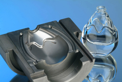
Aachen, Germany | Posted on November 14th, 2009Jobs are in short supply, and yet some sectors have difficulty in finding suitable trainees for specialist tasks, such as polishing injection molds. The work is time-consuming and monotonous but requires highest levels of concentration, because any blemish in the mold can render it useless. A skilled worker may often need a whole week to polish a single metal mold. Up to now it has not been possible to use machines for this dreary work because they cannot get into the curved shapes.
Researchers at the Fraunhofer Institute for Laser Technology ILT in Aachen have developed a way of automating the polishing work: "We do not polish the surface by hand with grinding and polishing media. Instead we use a laser," explains Dr.-Ing. Edgar Willenborg, group leader at the ILT. "The laser beam melts the surface to a depth of about 50 to 100 micrometers. Surface tension ensures that the liquid metal flows evenly and solidifies smoothly." Like in conventional grinding and polishing, the process is repeated with increasing degrees of fineness. In the first stage the researchers melt the surface to a depth of about 100 micrometers, in further steps they gradually reduce the depth. "We can set the melting depth by means of various parameters: the laser output, the speed at which the laser beam travels along the surface and the length of the laser pulses," states Willenborg. Laser polishing does not achieve the same surface smoothness as perfect hand polishing - hand polishers can achieve a roughness Ra of 5 nanometers, the laser at present can only manage 50 nanometers - but Willenborg still sees considerable market potential for the system. "We will concentrate on automating the medium grades: a roughness of 50 nanometers is adequate for many applications, including the molds used for making standard plastic parts." The high-end levels of smoothness will therefore remain the domain of skilled hand polishers.
The time gained by laser polishing and the cost saving achieved are enormous. Whereas a skilled polisher needs about 10 to 30 minutes for each square centimeter, the laser polishes the same area in about a minute. A prototype of the laser polishing machine developed by the scientists in cooperation with mechanical engineering firm Maschinenfabrik Arnold has already been built.
Willenborg estimates that the system will be ready for industrial use in one to two years' time. At the Euromold trade show, to be held from December 2 to 5 in Frankfurt, the researchers will be presenting examples of three-dimensional surfaces polished by laser (Hall 8, Stand M114).
####
About Fraunhofer-Gesellschaft
60 years ago, on March 26, 1949, the Fraunhofer-Gesellschaft was founded in the large conference hall of the Bavarian Ministry of the Economy. At the time, the idea was to develop new structures for research after the war's destruction, and to spur reconstruction of the economy.
For more information, please click here
Contacts:
Dr.-Ing. Edgar Willenborg
Fraunhofer-Institut f�r Lasertechnik (ILT)
Steinbachstr. 15
52074 Aachen
Phone 0241/8906-213
Copyright © Fraunhofer-Gesellschaft
If you have a comment, please Contact us.Issuers of news releases, not 7th Wave, Inc. or Nanotechnology Now, are solely responsible for the accuracy of the content.
Bookmark:


| Related News Press |
News and information
![]() Simulating magnetization in a Heisenberg quantum spin chain April 5th, 2024
Simulating magnetization in a Heisenberg quantum spin chain April 5th, 2024
![]() NRL charters Navy�s quantum inertial navigation path to reduce drift April 5th, 2024
NRL charters Navy�s quantum inertial navigation path to reduce drift April 5th, 2024
![]() Discovery points path to flash-like memory for storing qubits: Rice find could hasten development of nonvolatile quantum memory April 5th, 2024
Discovery points path to flash-like memory for storing qubits: Rice find could hasten development of nonvolatile quantum memory April 5th, 2024
Jobs
![]() Could quantum technology be New Mexico�s next economic boon? Quantum New Mexico Coalition aims to establish state as national hub April 1st, 2022
Could quantum technology be New Mexico�s next economic boon? Quantum New Mexico Coalition aims to establish state as national hub April 1st, 2022
![]() SEMI Partners with GLOBALFOUNDRIES to Offer Apprenticeship Program Aimed at Building the Electronics Talent Pipeline August 11th, 2020
SEMI Partners with GLOBALFOUNDRIES to Offer Apprenticeship Program Aimed at Building the Electronics Talent Pipeline August 11th, 2020
![]() Arrowhead Pharmaceuticals Reports Inducement Grants under NASDAQ Marketplace Rule 5635(c)(4) March 29th, 2019
Arrowhead Pharmaceuticals Reports Inducement Grants under NASDAQ Marketplace Rule 5635(c)(4) March 29th, 2019
Announcements
![]() NRL charters Navy�s quantum inertial navigation path to reduce drift April 5th, 2024
NRL charters Navy�s quantum inertial navigation path to reduce drift April 5th, 2024
![]() Discovery points path to flash-like memory for storing qubits: Rice find could hasten development of nonvolatile quantum memory April 5th, 2024
Discovery points path to flash-like memory for storing qubits: Rice find could hasten development of nonvolatile quantum memory April 5th, 2024
Industrial
![]() Boron nitride nanotube fibers get real: Rice lab creates first heat-tolerant, stable fibers from wet-spinning process June 24th, 2022
Boron nitride nanotube fibers get real: Rice lab creates first heat-tolerant, stable fibers from wet-spinning process June 24th, 2022
![]() Nanotubes: a promising solution for advanced rubber cables with 60% less conductive filler June 1st, 2022
Nanotubes: a promising solution for advanced rubber cables with 60% less conductive filler June 1st, 2022
![]() Protective equipment with graphene nanotubes meets the strictest ESD safety standards March 25th, 2022
Protective equipment with graphene nanotubes meets the strictest ESD safety standards March 25th, 2022
![]() OCSiAl receives the green light for Luxembourg graphene nanotube facility project to power the next generation of electric vehicles in Europe March 4th, 2022
OCSiAl receives the green light for Luxembourg graphene nanotube facility project to power the next generation of electric vehicles in Europe March 4th, 2022
Photonics/Optics/Lasers
![]() With VECSELs towards the quantum internet Fraunhofer: IAF achieves record output power with VECSEL for quantum frequency converters April 5th, 2024
With VECSELs towards the quantum internet Fraunhofer: IAF achieves record output power with VECSEL for quantum frequency converters April 5th, 2024
![]() Nanoscale CL thermometry with lanthanide-doped heavy-metal oxide in TEM March 8th, 2024
Nanoscale CL thermometry with lanthanide-doped heavy-metal oxide in TEM March 8th, 2024
![]() Optically trapped quantum droplets of light can bind together to form macroscopic complexes March 8th, 2024
Optically trapped quantum droplets of light can bind together to form macroscopic complexes March 8th, 2024
![]() HKUST researchers develop new integration technique for efficient coupling of III-V and silicon February 16th, 2024
HKUST researchers develop new integration technique for efficient coupling of III-V and silicon February 16th, 2024
|
|
||
|
|
||
| The latest news from around the world, FREE | ||
|
|
||
|
|
||
| Premium Products | ||
|
|
||
|
Only the news you want to read!
Learn More |
||
|
|
||
|
Full-service, expert consulting
Learn More |
||
|
|
||