Home > Press > Closest Look Ever at Graphene: Stunning Images of Individual Carbon Atoms From TEAM 0.5 microscope
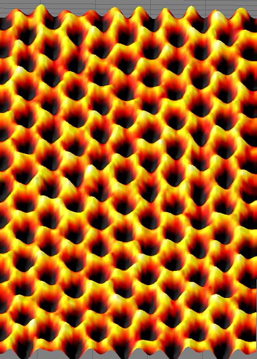 |
| This image of a single suspended sheet of graphene taken with TEAM 0.5, shows individual carbon atoms (yellow) on the honeycomb lattice. |
Abstract:
Hailed as the world's most powerful transmission electron microscope, TEAM 0.5 is living up to expectations. Using TEAM 0.5 (TEAM stands for Transmission Electron Aberration-corrected Microscope), researchers with the U.S. Department of Energy's Lawrence Berkeley National Laboratory (Berkeley Lab) have produced stunning images of individual carbon atoms in graphene, the two-dimensional crystalline form of carbon that is highly prized by the electronics industry.
Closest Look Ever at Graphene: Stunning Images of Individual Carbon Atoms From TEAM 0.5 microscope
Berkeley, CA | Posted on October 30th, 2009These first time ever images were recorded at Berkeley Lab's National Center for Electron Microscopy (NCEM), a DOE national user facility that is a premier center for electron microscopy and microcharacterization. TEAM 0.5, its newest instrument, is capable of producing images with half‑angstrom resolution, which is less than the diameter of a single hydrogen atom.
"Simply put, TEAM 0.5 is the best transmission electron microscope in the world, representing a quantum leap forward in instrumentation," said physicist Alex Zettl who led this research. "Having the ability to see, basically in real time, each and every individual atom in a sample is unbelievably useful and the images we can now see have been jaw-dropping for even the most seasoned electron microscopists. TEAM 0.5 is pushing transmission electron microscopy to a new level."
Zettl holds joint appointments with Berkeley Lab's Materials Sciences Division (MSD) and the Physics Department at the University of California's Berkeley campus, where he is the director of the Center of Integrated Nanomechanical Systems. Collaborating with him on this graphene imaging project were Jannik Meyer, also with Berkeley Lab's Materials Sciences Division, and Christian Kisielowski, Rolf Erni and Marta Rossell of NCEM.
Their results were published in the journal Nanoletters, in a paper entitled: "Direct imaging of lattice atoms and topological defects in graphene membranes."
The properties of solid materials stem from the arrangement of their constituent atoms in the solid's crystal structure. While technologies such as electron and x-ray crystallography can reveal the atomic geometry of a crystal, they do not identify the precise location and position of each individual atom. When the dimensions of a material shrink to the nanoscale, the location and position of each individual atom becomes critically important, as Zettl explains.
"Think of the steel re-bars on a three-dimensional structure, like a jungle gym," he said. "If a small piece of re-bar is rusted out somewhere in the center of the gym, it won't likely have much affect on the overall properties of the structure. In a two-dimensional structure, however, a rusted out segment becomes a much bigger problem, and in a one-dimensional structure, i.e., a single re-bar, a rusted out segment can be catastrophic, causing the entire structure to fail. On a nanoscale crystal, one missing atom or some other defect in the arrangement can result in catastrophic failure."
Graphene is especially sensitive to defects in its atomic structure. Consisting of a single-layered sheet of carbon atoms arranged in hexagons, like a sheet of chicken wire with an atom at each nexus, graphene features extraordinary electrical, mechanical and thermal properties that could enable it to serve in a broad array of carbon-based electronic devices. For the enormous promises of graphene to be fulfilled, however, scientists need a much better understanding of how specific types of defects in the crystal structure, including those that change location over time, affect its properties.
"Theorists are currently making all kinds of predictions about the properties of graphene for different local atomic configurations, but until TEAM 0.5, we did not have the ability to actually see and study these configurations in real time," Zettl said.
TEAM 0.5 features state-of-the-art technical advances including an extremely bright electron source, ultra-stable electronics to reduce drift and, perhaps most importantly, the ability to provide optical corrections for spherical aberration (blurring). By making points of light look like disks, spherical aberrations have been the prime limiting factors in the resolution of transmission electron microscopy.
Says NCEM principal investigator and collaborator on this study Kisielowski, "TEAM 0.5 allows for the detection of every single atom from the Periodic Table provided that the sample under investigation can stand the radiation damage (TEAM 0.5's record-setting half-angstrom resolution was achieved with an electron beam that was 300 kilovolts (kV) in energy.)
Correcting spherical aberration makes it possible to use the TEAM 0.5 not only for broad-beam "wide-angle" images but also for scanning transmission electron microscopy (STEM), in which the tightly focused electron beam is moved across a sample as a probe. In this mode, TEAM 0.5 is capable of performing spectroscopy on one atom at a time � an ideal way to precisely locate impurities in an otherwise homogeneous sample, such as individual dopant atoms in a semiconductor. Aberration correction also enables TEAM 0.5 to produce high resolution images at relatively low electron beam energies. Because of their longer wavelengths, lower energy electrons are more difficult to focus than higher energy electrons. Aberration correction overcomes this problem.
Using TEAM 0.5, Zettl, Kisielowski and their collaborators were able to obtain images of graphene membranes - crystalline foils one atom thick - at a resolution of one angstrom using electron beams of a mere 80 kilovolts (kV) in energy.
"The low voltage was crucial for the stability and study of these graphene membranes which are much too fragile to be imaged at the higher energies required for conventional transmission electron microscopy," said Zettl. "That we were able to detect and resolve every individual carbon atom in these foils at 80kV is relevant for future studies of organic materials where low-z atoms dominate and higher energies are damaging to samples. TEAM 0.5 provides fantastic resolution at low electron energies, which is the best of both worlds for organics."
Added Kisielowski, "This is not even the end of the story. We have since made improvements to further boost signal-to-noise ratios and already have new and even better images. There is much more to come."
TEAM 0.5 was designed and constructed through a collaboration led by Berkeley Lab and including DOE's Argonne and Oak Ridge National Laboratories, the Frederick Seitz Materials Laboratory of the University of Illinois, and two private companies specializing in electron microscopy, the FEI Company headquartered in Portland, Oregon, and CEOS of Heidelberg, Germany.
Additional Information
To view an advanced copy of the paper "Direct imaging of lattice atoms and topological defects in graphene membranes" which is now available on-line in the journal Nanoletters here:
pubs.acs.org/cgi-bin/asap.cgi/nalefd/asap/pdf/nl801386m.pdf
To learn more about Alex Zettl and his research group here: www.physics.berkeley.edu/research/zettl/
To learn more about TEAM 05. and the National Center for Electron Microscopy here ncem.lbl.gov/
####
About Lawrence Berkeley National Laboratory
In the world of science, Lawrence Berkeley National Laboratory (Berkeley Lab) is synonymous with �excellence.� Eleven scientists associated with Berkeley Lab have won the Nobel Prize and 55 Nobel Laureates either trained here or had significant collaborations with our Laboratory. Thirteen of our scientists have won the National Medal of Science, our nation's highest award for lifetime achievement in fields of scientific research. As of 2008, there have been 61 Berkeley Lab scientists elected into the National Academy of Sciences (NAS), considered one of the highest honors for a scientist in the United States. This translates to approximately three-percent of the total NAS membership, an unparalleled record of achievement. Eighteen of our engineers have been elected to the National Academy of Engineering, and two of our scientists have been elected into the Institute of Medicine. In addition, Berkeley Lab has trained thousands of university science and engineering students who are advancing technological innovations across the nation and around the world.
For more information, please click here
Contacts:
Lynn Yarris
(510) 486-5375
Copyright © Lawrence Berkeley National Laboratory
If you have a comment, please Contact us.Issuers of news releases, not 7th Wave, Inc. or Nanotechnology Now, are solely responsible for the accuracy of the content.
Bookmark:


| Related News Press |
Announcements
![]() A fundamentally new therapeutic approach to cystic fibrosis: Nanobody repairs cellular defect April 17th, 2026
A fundamentally new therapeutic approach to cystic fibrosis: Nanobody repairs cellular defect April 17th, 2026
![]() UC Irvine physicists discover method to reverse �quantum scrambling� : The work addresses the problem of information loss in quantum computing system April 17th, 2026
UC Irvine physicists discover method to reverse �quantum scrambling� : The work addresses the problem of information loss in quantum computing system April 17th, 2026
Tools
![]() Metasurfaces smooth light to boost magnetic sensing precision January 30th, 2026
Metasurfaces smooth light to boost magnetic sensing precision January 30th, 2026
![]() From sensors to smart systems: the rise of AI-driven photonic noses January 30th, 2026
From sensors to smart systems: the rise of AI-driven photonic noses January 30th, 2026
![]() Japan launches fully domestically produced quantum computer: Expo visitors to experience quantum computing firsthand August 8th, 2025
Japan launches fully domestically produced quantum computer: Expo visitors to experience quantum computing firsthand August 8th, 2025
|
|
||
|
|
||
| The latest news from around the world, FREE | ||
|
|
||
|
|
||
| Premium Products | ||
|
|
||
|
Only the news you want to read!
Learn More |
||
|
|
||
|
Full-service, expert consulting
Learn More |
||
|
|
||