Home > Press > Applied Materials Opens Advanced Solar Research and Customer Demonstration Facility in Xi’an, China
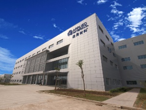 |
| Applied Materials opened the world's largest solar R&D and customer demonstration facility in Xi'an, China on October 26. The state-of-the-art facility houses complete crystalline silicon and SunFab thin film pilot production lines. (Photo: Business Wire) |
Abstract:
Applied Materials, Inc. the world's largest supplier of equipment to the solar photovoltaic industry, today opened an advanced solar research and demonstration facility in Xi'an, China. Applied Materials' Solar Technology Center, the largest non-government solar energy research facility in the world, is comprised of laboratory and office buildings covering more than 400,000 square feet and contains an entire Applied SunFab™ thin film manufacturing line and a complete crystalline silicon pilot process. These lines are configured to closely simulate customer fabrication (fab) environments.
Applied Materials Opens Advanced Solar Research and Customer Demonstration Facility in Xi’an, China
XI’AN, China | Posted on October 26th, 2009"This opening represents a critical breakthrough for the photovoltaic industry and China and a tremendous benefit to our customers," said Mike Splinter, chairman and CEO of Applied Materials. "Establishing this center in China is an integral part of Applied's global strategy and an important step toward the industrialization of the global solar industry."
Applied Materials is celebrating its 25th anniversary in China this year and today has more than 800 employees and 13 offices in the country, with approximately 300 employees in Xi'an. Applied first broke ground in Xi'an in 2006 and the total investment in the multi-phase project is more than $250 million dollars. The completed facility includes a solar technology center for R&D, engineering, product demonstration, testing and training for crystalline silicon and thin film solar module manufacturing equipment and processes. Employees in the center will work closely with local suppliers to test and qualify new materials and tools and evaluate potential new cost saving technologies. The center has the largest solar array in Xi'an, a 56 kW array on a parking lot structure.
"We believe this technology center will provide important contributions to driving down the cost of solar around the world," stated Mark Pinto, senior vice president, general manager, Energy and Environmental Solutions and Applied's chief technology officer. "In addition to housing Applied's state-of-the-art research into solar manufacturing techniques, customers and potential customers from around the world will be able to work side-by-side with our technologists to reduce their time to market and improve factory productivity and cell efficiency."
Xi'an is located in the Shaanxi province in northwest China and is a growing center of energy technology excellence in China. The local province boasts more than 40 colleges and universities and Xi'an is recognized as one of the leading high-technology research areas in the country. Applied has worked closely with local governments, contributed to research and awarded 166 university scholarships since 2005 through an R&D fund with the Xi'an Municipal Science and Technology Commission and Xi'an High Tech Park.
"As China works to build its renewable power infrastructure we are pleased to offer such a unique facility. In the laboratories, local suppliers of systems and materials will be able to work closely with our engineers to reduce development costs, accelerate the industrialization of clean energy technology and contribute to decreasing the cost of solar," said Charlie Gay, president, Applied Solar. "This is a powerful benefit we are bringing to our customers and to China, and we look forward to immediately putting these capabilities to work."
####
About Applied Materials
Applied Materials, Inc. (Nasdaq:AMAT) is the global leader in Nanomanufacturing Technology™ solutions with a broad portfolio of innovative equipment, service and software products for the fabrication of semiconductor chips, flat panel displays, solar photovoltaic cells, flexible electronics and energy efficient glass. At Applied Materials, we apply Nanomanufacturing Technology to improve the way people live.
For more information, please click here
Contacts:
Applied Materials, Inc.
David Miller, 408-563-9582 (editorial/media)
Michael Sullivan, 408-986-7977 (financial community)
Copyright © Businesswire
If you have a comment, please Contact us.Issuers of news releases, not 7th Wave, Inc. or Nanotechnology Now, are solely responsible for the accuracy of the content.
Bookmark:


| Related News Press |
News and information
![]() Quantum computer improves AI predictions April 17th, 2026
Quantum computer improves AI predictions April 17th, 2026
![]() Flexible sensor gains sensitivity under pressure April 17th, 2026
Flexible sensor gains sensitivity under pressure April 17th, 2026
![]() A reusable chip for particulate matter sensing April 17th, 2026
A reusable chip for particulate matter sensing April 17th, 2026
![]() Detecting vibrational quantum beating in the predissociation dynamics of SF6 using time-resolved photoelectron spectroscopy April 17th, 2026
Detecting vibrational quantum beating in the predissociation dynamics of SF6 using time-resolved photoelectron spectroscopy April 17th, 2026
Thin films
![]() Tiny nanosheets, big leap: A new sensor detects ethanol at ultra-low levels January 30th, 2026
Tiny nanosheets, big leap: A new sensor detects ethanol at ultra-low levels January 30th, 2026
![]() Utilizing palladium for addressing contact issues of buried oxide thin film transistors April 5th, 2024
Utilizing palladium for addressing contact issues of buried oxide thin film transistors April 5th, 2024
![]() Understanding the mechanism of non-uniform formation of diamond film on tools: Paving the way to a dry process with less environmental impact March 24th, 2023
Understanding the mechanism of non-uniform formation of diamond film on tools: Paving the way to a dry process with less environmental impact March 24th, 2023
![]() New study introduces the best graphite films: The work by Distinguished Professor Feng Ding at UNIST has been published in the October 2022 issue of Nature Nanotechnology November 4th, 2022
New study introduces the best graphite films: The work by Distinguished Professor Feng Ding at UNIST has been published in the October 2022 issue of Nature Nanotechnology November 4th, 2022
Jobs
![]() Could quantum technology be New Mexico’s next economic boon? Quantum New Mexico Coalition aims to establish state as national hub April 1st, 2022
Could quantum technology be New Mexico’s next economic boon? Quantum New Mexico Coalition aims to establish state as national hub April 1st, 2022
![]() SEMI Partners with GLOBALFOUNDRIES to Offer Apprenticeship Program Aimed at Building the Electronics Talent Pipeline August 11th, 2020
SEMI Partners with GLOBALFOUNDRIES to Offer Apprenticeship Program Aimed at Building the Electronics Talent Pipeline August 11th, 2020
![]() Arrowhead Pharmaceuticals Reports Inducement Grants under NASDAQ Marketplace Rule 5635(c)(4) March 29th, 2019
Arrowhead Pharmaceuticals Reports Inducement Grants under NASDAQ Marketplace Rule 5635(c)(4) March 29th, 2019
Announcements
![]() A fundamentally new therapeutic approach to cystic fibrosis: Nanobody repairs cellular defect April 17th, 2026
A fundamentally new therapeutic approach to cystic fibrosis: Nanobody repairs cellular defect April 17th, 2026
![]() UC Irvine physicists discover method to reverse ‘quantum scrambling’ : The work addresses the problem of information loss in quantum computing system April 17th, 2026
UC Irvine physicists discover method to reverse ‘quantum scrambling’ : The work addresses the problem of information loss in quantum computing system April 17th, 2026
Industrial
![]() Tiny nanosheets, big leap: A new sensor detects ethanol at ultra-low levels January 30th, 2026
Tiny nanosheets, big leap: A new sensor detects ethanol at ultra-low levels January 30th, 2026
![]() Quantum interference in molecule-surface collisions February 28th, 2025
Quantum interference in molecule-surface collisions February 28th, 2025
![]() Boron nitride nanotube fibers get real: Rice lab creates first heat-tolerant, stable fibers from wet-spinning process June 24th, 2022
Boron nitride nanotube fibers get real: Rice lab creates first heat-tolerant, stable fibers from wet-spinning process June 24th, 2022
Alliances/Trade associations/Partnerships/Distributorships
![]() Chicago Quantum Exchange welcomes six new partners highlighting quantum technology solutions, from Chicago and beyond September 23rd, 2022
Chicago Quantum Exchange welcomes six new partners highlighting quantum technology solutions, from Chicago and beyond September 23rd, 2022
![]() University of Illinois Chicago joins Brookhaven Lab's Quantum Center June 10th, 2022
University of Illinois Chicago joins Brookhaven Lab's Quantum Center June 10th, 2022
Solar/Photovoltaic
![]() Spinel-type sulfide semiconductors to operate the next-generation LEDs and solar cells For solar-cell absorbers and green-LED source October 3rd, 2025
Spinel-type sulfide semiconductors to operate the next-generation LEDs and solar cells For solar-cell absorbers and green-LED source October 3rd, 2025
![]() KAIST researchers introduce new and improved, next-generation perovskite solar cell November 8th, 2024
KAIST researchers introduce new and improved, next-generation perovskite solar cell November 8th, 2024
![]() Groundbreaking precision in single-molecule optoelectronics August 16th, 2024
Groundbreaking precision in single-molecule optoelectronics August 16th, 2024
![]() Development of zinc oxide nanopagoda array photoelectrode: photoelectrochemical water-splitting hydrogen production January 12th, 2024
Development of zinc oxide nanopagoda array photoelectrode: photoelectrochemical water-splitting hydrogen production January 12th, 2024
|
|
||
|
|
||
| The latest news from around the world, FREE | ||
|
|
||
|
|
||
| Premium Products | ||
|
|
||
|
Only the news you want to read!
Learn More |
||
|
|
||
|
Full-service, expert consulting
Learn More |
||
|
|
||