Home > Press > NIST Scientists Study How to Stack the Deck for Organic Solar Power
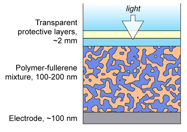 |
| In this cross-section of an organic photovoltaic cell, light passes through the upper layers (from top down, glass, indium tin dioxide, and thermoplastic) and generates a photocurrent in the polymer-fullerene layer. Channels formed by polymers (tan) and fullerenes (dark blue) allow electric current to flow into the electrode at bottom. NIST research has revealed new information about how the channels form, potentially improving cell performance. Credit: NIST |
Abstract:
A new class of economically viable solar power cells—cheap, flexible and easy to make—has come a step closer to reality as a result of recent work* at the National Institute of Standards and Technology (NIST), where scientists have deepened their understanding of the complex organic films at the heart of the devices.
NIST Scientists Study How to Stack the Deck for Organic Solar Power
Gaithersburg, MD | Posted on August 5th, 2009Organic photovoltaics, which rely on organic molecules to capture sunlight and convert it into electricity, are a hot research area because in principle they have significant advantages over traditional rigid silicon cells. Organic photovoltaics start out as a kind of ink that can be applied to flexible surfaces to create solar cell modules that can be spread over large areas as easily as unrolling a carpet. They'd be much cheaper to make and easier to adapt to a wide variety of power applications, but their market share will be limited until the technology improves. Even the best organic photovoltaics convert less than 6 percent of light into electricity and last only a few thousand hours. "The industry believes that if these cells can exceed 10 percent efficiency and 10,000 hours of life, technology adoption will really accelerate," says NIST's David Germack. "But to improve them, there is critical need to identify what's happening in the material, and at this point, we're only at the beginning."
The NIST team has advanced that understanding with their latest effort, which provides a powerful new measurement strategy for organic photovoltaics that reveals ways to control how they form. In the most common class of organic photovoltaics, the "ink" is a blend of a polymer that absorbs sunlight, enabling it to give up its electrons, and ball-shaped carbon molecules called fullerenes that collect electrons. When the ink is applied to a surface, the blend hardens into a film that contains a haphazard network of polymers intermixed with fullerene channels. In conventional devices, the polymer network should ideally all reach the bottom of the film while the fullerene channels should ideally all reach the top, so that electricity can flow in the correct direction out of the device. However, if barriers of fullerenes form between the polymers and the bottom edge of the film, the cell's efficiency will be reduced.
By applying X-ray absorption measurements to the film interfaces, the team discovered that by changing the nature of the electrode surface, it will repulse fullerenes (like oil repulses water) while attracting the polymer. The electrical properties of the interface also change dramatically. The resultant structure gives the light-generated photocurrent more opportunities to reach the proper electrodes and reduces the accumulation of fullerenes at the film bottom, both of which could improve the photovoltaic's efficiency or lifetime.
"We've identified some key parameters needed to optimize what happens at both edges of the film, which means the industry will have a strategy to optimize the cell's overall performance," Germack says. "Right now, we're building on what we've learned about the edges to identify what happens throughout the film. This knowledge is really important to help industry figure out how organic cells perform and age so that their life spans will be extended."
* D.S. Germack, C.K. Chan, B.H. Hamadani, L.J. Richter, D.A. Fischer, D.J. Gundlach and D.M. DeLongchamp. Substrate-dependent interface composition and charge transport in films for organic photovoltaics. Applied Physics Letters, 94, 233303 (2009), DOI: 10.1063/1.3149706.
####
About National Institute of Standards and Technology
From automated teller machines and atomic clocks to mammograms and semiconductors, innumerable products and services rely in some way on technology, measurement, and standards provided by the National Institute of Standards and Technology.
Founded in 1901, NIST is a non-regulatory federal agency within the U.S. Department of Commerce. NIST's mission is to promote U.S. innovation and industrial competitiveness by advancing measurement science, standards, and technology in ways that enhance economic security and improve our quality of life.
For more information, please click here
Contacts:
Media Contact
Chad Boutin
(301) 975-4261
Copyright © National Institute of Standards and Technology
If you have a comment, please Contact us.Issuers of news releases, not 7th Wave, Inc. or Nanotechnology Now, are solely responsible for the accuracy of the content.
Bookmark:


| Related News Press |
News and information
![]() Simulating magnetization in a Heisenberg quantum spin chain April 5th, 2024
Simulating magnetization in a Heisenberg quantum spin chain April 5th, 2024
![]() NRL charters Navy’s quantum inertial navigation path to reduce drift April 5th, 2024
NRL charters Navy’s quantum inertial navigation path to reduce drift April 5th, 2024
![]() Discovery points path to flash-like memory for storing qubits: Rice find could hasten development of nonvolatile quantum memory April 5th, 2024
Discovery points path to flash-like memory for storing qubits: Rice find could hasten development of nonvolatile quantum memory April 5th, 2024
![]() Good as gold - improving infectious disease testing with gold nanoparticles April 5th, 2024
Good as gold - improving infectious disease testing with gold nanoparticles April 5th, 2024
Thin films
![]() Utilizing palladium for addressing contact issues of buried oxide thin film transistors April 5th, 2024
Utilizing palladium for addressing contact issues of buried oxide thin film transistors April 5th, 2024
![]() Understanding the mechanism of non-uniform formation of diamond film on tools: Paving the way to a dry process with less environmental impact March 24th, 2023
Understanding the mechanism of non-uniform formation of diamond film on tools: Paving the way to a dry process with less environmental impact March 24th, 2023
![]() New study introduces the best graphite films: The work by Distinguished Professor Feng Ding at UNIST has been published in the October 2022 issue of Nature Nanotechnology November 4th, 2022
New study introduces the best graphite films: The work by Distinguished Professor Feng Ding at UNIST has been published in the October 2022 issue of Nature Nanotechnology November 4th, 2022
Possible Futures
![]() Discovery points path to flash-like memory for storing qubits: Rice find could hasten development of nonvolatile quantum memory April 5th, 2024
Discovery points path to flash-like memory for storing qubits: Rice find could hasten development of nonvolatile quantum memory April 5th, 2024
![]() With VECSELs towards the quantum internet Fraunhofer: IAF achieves record output power with VECSEL for quantum frequency converters April 5th, 2024
With VECSELs towards the quantum internet Fraunhofer: IAF achieves record output power with VECSEL for quantum frequency converters April 5th, 2024
Announcements
![]() NRL charters Navy’s quantum inertial navigation path to reduce drift April 5th, 2024
NRL charters Navy’s quantum inertial navigation path to reduce drift April 5th, 2024
![]() Discovery points path to flash-like memory for storing qubits: Rice find could hasten development of nonvolatile quantum memory April 5th, 2024
Discovery points path to flash-like memory for storing qubits: Rice find could hasten development of nonvolatile quantum memory April 5th, 2024
Energy
![]() Development of zinc oxide nanopagoda array photoelectrode: photoelectrochemical water-splitting hydrogen production January 12th, 2024
Development of zinc oxide nanopagoda array photoelectrode: photoelectrochemical water-splitting hydrogen production January 12th, 2024
![]() Shedding light on unique conduction mechanisms in a new type of perovskite oxide November 17th, 2023
Shedding light on unique conduction mechanisms in a new type of perovskite oxide November 17th, 2023
![]() Inverted perovskite solar cell breaks 25% efficiency record: Researchers improve cell efficiency using a combination of molecules to address different November 17th, 2023
Inverted perovskite solar cell breaks 25% efficiency record: Researchers improve cell efficiency using a combination of molecules to address different November 17th, 2023
![]() The efficient perovskite cells with a structured anti-reflective layer – another step towards commercialization on a wider scale October 6th, 2023
The efficient perovskite cells with a structured anti-reflective layer – another step towards commercialization on a wider scale October 6th, 2023
Solar/Photovoltaic
![]() Development of zinc oxide nanopagoda array photoelectrode: photoelectrochemical water-splitting hydrogen production January 12th, 2024
Development of zinc oxide nanopagoda array photoelectrode: photoelectrochemical water-splitting hydrogen production January 12th, 2024
![]() Shedding light on unique conduction mechanisms in a new type of perovskite oxide November 17th, 2023
Shedding light on unique conduction mechanisms in a new type of perovskite oxide November 17th, 2023
![]() Inverted perovskite solar cell breaks 25% efficiency record: Researchers improve cell efficiency using a combination of molecules to address different November 17th, 2023
Inverted perovskite solar cell breaks 25% efficiency record: Researchers improve cell efficiency using a combination of molecules to address different November 17th, 2023
![]() Charged “molecular beasts” the basis for new compounds: Researchers at Leipzig University use “aggressive” fragments of molecular ions for chemical synthesis November 3rd, 2023
Charged “molecular beasts” the basis for new compounds: Researchers at Leipzig University use “aggressive” fragments of molecular ions for chemical synthesis November 3rd, 2023
|
|
||
|
|
||
| The latest news from around the world, FREE | ||
|
|
||
|
|
||
| Premium Products | ||
|
|
||
|
Only the news you want to read!
Learn More |
||
|
|
||
|
Full-service, expert consulting
Learn More |
||
|
|
||