Home > Press > Carl Zeiss Launches Next-Generation Analytical Electron Microscope
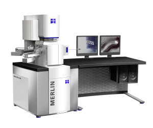 |
| A key aspect of the new FE-SEM MERLIN(TM) from Carl Zeiss is Ease of use, for example in-situ sample cleaning, unique charge compensation or image acquisition in less than one minute. (Graphic: Business Wire) |
Abstract:
Today Carl Zeiss announces a series of launches covering a range of product and application innovations.
Carl Zeiss Launches Next-Generation Analytical Electron Microscope
Germany | Posted on July 1st, 2009The start of this series is marked by the next-generation analytical field emission scanning electron microscope - the MERLIN�. This instrument combines the up to now contradictory requirements of ultra-high resolution imaging and analytical capabilities. "Customers have a need for more than just high resolution images of their samples," Dr. Dirk Stenkamp, Member of the Board at Carl Zeiss SMT explains. "With unique analytical capabilities our instruments provide maximum information with maximum insight."
MERLIN� - analysis and high resolution in one
The MERLIN FE-SEM overcomes the conflict between image resolution and analytical capability. The core of MERLIN is the enhanced GEMINI II column which, with its double condenser system, achieves an image resolution of 0.8 nanometers. A sample current of up to 300 nanoamperes is available for analytical purposes such as energy and wavelength dispersive X-ray spectroscopy (EDS and WDS), diffraction analysis of backscattered electrons (EBSD) or the generation of cathodoluminescence.
The system supports the user with a wide range of detailed solutions for tasks that could not be adequately performed in the past. The foundation for this achievement has been laid by the Carl Zeiss "Complete Detection System". This consists of the in-lens SE detector for surface imaging, the in-lens EsB detector for material contrast and the AsB detector for widely dispersed backscattered electrons. The latter contain specific information on the crystal orientation of the sample.
The unique charge compensation system of MERLIN also allows the high-resolution imaging of non-conductive samples. Electrons, which accumulate on the surface of the sample, are swept away by a fine jet of nitrogen. In doing so, the complete detection system of MERLIN can be used. An additional feature of the system for charge compensation is a channel for pure oxygen enabling in-situ sample cleaning. Within the vacuum chamber frequently occurring carbon deposits are removed from the sample surface, thus producing a significantly crisper and contrasty image. Both options allow the user to concentrate on the imaging and analysis of the sample instead of investing time and money in sample preparation.
MERLIN's new electronic system permits a flexible instrument configuration. Additional detectors can be retrofitted quickly, allowing the user to adapt the system to growing requirements. In addition, this flexibility makes the investment more future-proof and enables the user to benefit over the long term from ongoing detector development.
"The new MERLIN, as well as the just recently introduced AURIGA CrossBeam workstation perfectly embody what our products stand for: Maximum Information - Maximum Insight", Stenkamp points out. "And - the market can expect much more in the coming weeks until M&M show and the European Microscopy Conference in Graz, Austria, end of August."
####
About Carl Zeiss
Carl Zeiss SMT utilizes its globally leading know-how in light, electron and ion-optical technologies to offer its customers in industry and R&D a broad portfolio of products, services and application solutions. The market-leading systems and solutions from Carl Zeiss SMT are used in mutually strengthening fields of application in nanotechnology such as semiconductor technology, materials research and the life sciences. The global customer community is constantly growing. As the innovation leader for lithography optics, as well as optical and particle-beam based inspection, analysis and measuring systems, Carl Zeiss SMT opens up new avenues for its customers in industrial manufacturing environments, quality assurance and industrial and university R&D.
Together with its subsidiaries in Germany, England, France, the USA, Israel and Singapore, the international group of companies has over 2,500 employees. In fiscal year 2007/08, the wholly owned subsidiary of Carl Zeiss AG generated revenues of over EUR 1,000 million.
For more information, please click here
Contacts:
Carl Zeiss SMT AG, GermanyMarkus Wiederspahn
+49 73 64 20 21 94
Public Relations
Zeiss SMT, Inc., MABill Monigle,
941-497-1622
Public Relations, North America
Copyright © Business Wire
If you have a comment, please Contact us.Issuers of news releases, not 7th Wave, Inc. or Nanotechnology Now, are solely responsible for the accuracy of the content.
Bookmark:


| Related News Press |
News and information
![]() Quantum computer improves AI predictions April 17th, 2026
Quantum computer improves AI predictions April 17th, 2026
![]() Flexible sensor gains sensitivity under pressure April 17th, 2026
Flexible sensor gains sensitivity under pressure April 17th, 2026
![]() A reusable chip for particulate matter sensing April 17th, 2026
A reusable chip for particulate matter sensing April 17th, 2026
![]() Detecting vibrational quantum beating in the predissociation dynamics of SF6 using time-resolved photoelectron spectroscopy April 17th, 2026
Detecting vibrational quantum beating in the predissociation dynamics of SF6 using time-resolved photoelectron spectroscopy April 17th, 2026
Announcements
![]() A fundamentally new therapeutic approach to cystic fibrosis: Nanobody repairs cellular defect April 17th, 2026
A fundamentally new therapeutic approach to cystic fibrosis: Nanobody repairs cellular defect April 17th, 2026
![]() UC Irvine physicists discover method to reverse �quantum scrambling� : The work addresses the problem of information loss in quantum computing system April 17th, 2026
UC Irvine physicists discover method to reverse �quantum scrambling� : The work addresses the problem of information loss in quantum computing system April 17th, 2026
Tools
![]() Metasurfaces smooth light to boost magnetic sensing precision January 30th, 2026
Metasurfaces smooth light to boost magnetic sensing precision January 30th, 2026
![]() From sensors to smart systems: the rise of AI-driven photonic noses January 30th, 2026
From sensors to smart systems: the rise of AI-driven photonic noses January 30th, 2026
![]() Japan launches fully domestically produced quantum computer: Expo visitors to experience quantum computing firsthand August 8th, 2025
Japan launches fully domestically produced quantum computer: Expo visitors to experience quantum computing firsthand August 8th, 2025
|
|
||
|
|
||
| The latest news from around the world, FREE | ||
|
|
||
|
|
||
| Premium Products | ||
|
|
||
|
Only the news you want to read!
Learn More |
||
|
|
||
|
Full-service, expert consulting
Learn More |
||
|
|
||