Home > Press > Remote Demos of JEOL Analytical SEM at Semicon
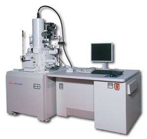 |
| JEOL JSM-7600F Analytical FE SEM |
Abstract:
JEOL to Remotely Demonstrate New High Throughput, Ultrahigh Resolution Analytical FE SEM at Semicon West 2009
Remote Demos of JEOL Analytical SEM at Semicon
Peabody, MA | Posted on June 30th, 2009JEOL, a leading supplier of electron microscopes for ultrahigh resolution imaging and analysis, will demonstrate its new ultrahigh resolution, analytical Thermal Field Emission Scanning Electron Microscope (SEM), the JSM-7600F, via live remote viewing and control from Semicon West, San Francisco, July 14-16.
The SEM will be remotely operated from JEOL's booth #606 to demonstrate ultrahigh imaging resolution at up to 1,000,000X magnification, and X-ray analytical mapping of individual layers, elemental composition, contaminants, particulates, and process defects in semiconductor devices.
The only fully-analytical field emission SEM to feature a large chamber with large specimen exchange airlock and LN2 anti-contaminator, the JSM-7600F accommodates specimens up to 200mm in diameter, and features a highly stable 5-axis motor drive eucentric stage that can be tilted from -5 to 70o.
The microscope's electron column produces the highest beam current available on any FEG SEM, and provides superior imaging of nonconductive samples that traditionally charge. The JSM-7600F minimizes beam damage on heat sensitive samples, i.e. low-K dielectrics, and offers improved stability for unattended data acquisition, particle analysis, EBSD, and X-ray mapping.
The JEOL JSM-7600F is fully outfitted for comprehensive analysis techniques and can simultaneously view and acquire images and data from four different types of imaging detectors. The SEM also does double duty as a direct write e-beam lithography tool when outfitted with a high speed beam blanker and a pattern generator (see previous release at www.jeolusa.com/NEWSEVENTS/PressReleases/tabid/314/newsid735/148/West-Virginia-University-Advancing-Nanoscience-with-New-E-beam-SEM/Default.aspx)
####
About JEOL
Since 1949, the JEOL legacy has been one of outstanding innovation in developing instruments used to advance scientific research and technology. JEOL has 60 years of expertise in the field of electron microscopy, more than 50 years in mass spectrometry and NMR spectrometry, and more than 40 years of e-beam lithography leadership.
JEOL USA, Inc., a wholly-owned subsidiary of JEOL Ltd. Japan, was incorporated in the United States in 1962. The primary business of JEOL USA is sales of new instruments and peripherals and support of a vast installed base of instruments throughout the United States, Canada, Mexico, and South America.
For more information, please click here
Contacts:
Patricia Corkum
Marketing Manager
JEOL USA
978-536-2273
Pamela Mansfield
Marketing Communications
JEOL USA
11 Dearborn Road
Peabody, MA 01966
Copyright © JEOL
If you have a comment, please Contact us.Issuers of news releases, not 7th Wave, Inc. or Nanotechnology Now, are solely responsible for the accuracy of the content.
Bookmark:


| Related News Press |
News and information
![]() Quantum computer improves AI predictions April 17th, 2026
Quantum computer improves AI predictions April 17th, 2026
![]() Flexible sensor gains sensitivity under pressure April 17th, 2026
Flexible sensor gains sensitivity under pressure April 17th, 2026
![]() A reusable chip for particulate matter sensing April 17th, 2026
A reusable chip for particulate matter sensing April 17th, 2026
![]() Detecting vibrational quantum beating in the predissociation dynamics of SF6 using time-resolved photoelectron spectroscopy April 17th, 2026
Detecting vibrational quantum beating in the predissociation dynamics of SF6 using time-resolved photoelectron spectroscopy April 17th, 2026
Announcements
![]() A fundamentally new therapeutic approach to cystic fibrosis: Nanobody repairs cellular defect April 17th, 2026
A fundamentally new therapeutic approach to cystic fibrosis: Nanobody repairs cellular defect April 17th, 2026
![]() UC Irvine physicists discover method to reverse �quantum scrambling� : The work addresses the problem of information loss in quantum computing system April 17th, 2026
UC Irvine physicists discover method to reverse �quantum scrambling� : The work addresses the problem of information loss in quantum computing system April 17th, 2026
Tools
![]() Metasurfaces smooth light to boost magnetic sensing precision January 30th, 2026
Metasurfaces smooth light to boost magnetic sensing precision January 30th, 2026
![]() From sensors to smart systems: the rise of AI-driven photonic noses January 30th, 2026
From sensors to smart systems: the rise of AI-driven photonic noses January 30th, 2026
![]() Japan launches fully domestically produced quantum computer: Expo visitors to experience quantum computing firsthand August 8th, 2025
Japan launches fully domestically produced quantum computer: Expo visitors to experience quantum computing firsthand August 8th, 2025
Events/Classes
![]() Institute for Nanoscience hosts annual proposal planning meeting May 16th, 2025
Institute for Nanoscience hosts annual proposal planning meeting May 16th, 2025
![]() A New Blue: Mysterious origin of the ribbontail ray�s electric blue spots revealed July 5th, 2024
A New Blue: Mysterious origin of the ribbontail ray�s electric blue spots revealed July 5th, 2024
![]() Researchers demonstrate co-propagation of quantum and classical signals: Study shows that quantum encryption can be implemented in existing fiber networks January 20th, 2023
Researchers demonstrate co-propagation of quantum and classical signals: Study shows that quantum encryption can be implemented in existing fiber networks January 20th, 2023
|
|
||
|
|
||
| The latest news from around the world, FREE | ||
|
|
||
|
|
||
| Premium Products | ||
|
|
||
|
Only the news you want to read!
Learn More |
||
|
|
||
|
Full-service, expert consulting
Learn More |
||
|
|
||