Home > Press > New 'broadband' cloaking technology simple to manufacture
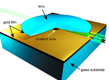 |
| This image shows the design of a new type of invisibility cloak that is simpler than previous designs and works for all colors of the visible spectrum, making it possible to cloak larger objects than before and possibly leading to practical applications in "transformation optics." (Purdue University) |
Abstract:
Anisotropic Metamaterials Emulated
by Tapered Waveguides:
Application to Optical Cloaking
Igor I. Smolyaninov1, Vera N. Smolyaninova2, Alexander V. Kildishev3, and Vladimir M. Shalaev3
1Advanced Technologies, BAE Systems, Washington, D.C.; 2Dept. of Physics Astronomy and Geosciences, Towson University; 3Birck Nanotechnology Center, School of Electrical and Computer Engineering, Purdue University
We demonstrate that metamaterial devices requiring anisotropic dielectric permittivity and magnetic permeability may be emulated by specially designed tapered waveguides. This approach leads to low-loss, broadband performance. Based on this technique, we demonstrate broadband electromagnetic cloaking in the visible frequency range on a scale ~100 times larger than the wavelength.
New 'broadband' cloaking technology simple to manufacture
WEST LAFAYETTE, IN | Posted on May 20th, 2009Researchers have created a new type of invisibility cloak that is simpler than previous designs and works for all colors of the visible spectrum, making it possible to cloak larger objects than before and possibly leading to practical applications in "transformation optics."
Whereas previous cloaking designs have used exotic "metamaterials," which require complex nanofabrication, the new design is a far simpler device based on a "tapered optical waveguide," said Vladimir Shalaev, Purdue University's Robert and Anne Burnett Professor of Electrical and Computer Engineering.
Waveguides represent established technology - including fiber optics - used in communications and other commercial applications.
The research team used their specially tapered waveguide to cloak an area 100 times larger than the wavelengths of light shined by a laser into the device, an unprecedented achievement. Previous experiments with metamaterials have been limited to cloaking regions only a few times larger than the wavelengths of visible light.
Because the new method enabled the researchers to dramatically increase the cloaked area, the technology offers hope of cloaking larger objects, Shalaev said.
Findings are detailed in a research paper appearing May 29 in the journal Physical Review Letters. The paper was written by Igor I. Smolyaninov, a principal electronic engineer at BAE Systems in Washington, D.C.; Vera N. Smolyaninova, an assistant professor of physics at Towson University in Maryland; Alexander Kildishev, a principal research scientist at Purdue's Birck Nanotechnology Center; and Shalaev.
"All previous attempts at optical cloaking have involved very complicated nanofabrication of metamaterials containing many elements, which makes it very difficult to cloak large objects," Shalaev said. "Here, we showed that if a waveguide is tapered properly it acts like a sophisticated nanostructured material."
The waveguide is inherently broadband, meaning it could be used to cloak the full range of the visible light spectrum. Unlike metamaterials, which contain many light-absorbing metal components, only a small portion of the new design contains metal.
Theoretical work for the design was led by Purdue, with BAE Systems leading work to fabricate the device, which is formed by two gold-coated surfaces, one a curved lens and the other a flat sheet. The researchers cloaked an object about 50 microns in diameter, or roughly the width of a human hair, in the center of the waveguide.
"Instead of being reflected as normally would happen, the light flows around the object and shows up on the other side, like water flowing around a stone," Shalaev said.
The research falls within a new field called transformation optics, which may usher in a host of radical advances, including cloaking; powerful "hyperlenses" resulting in microscopes 10 times more powerful than today's and able to see objects as small as DNA; computers and consumer electronics that use light instead of electronic signals to process information; advanced sensors; and more efficient solar collectors.
Unlike natural materials, metamaterials are able to reduce the "index of refraction" to less than one or less than zero. Refraction occurs as electromagnetic waves, including light, bend when passing from one material into another. It causes the bent-stick-in-water effect, which occurs when a stick placed in a glass of water appears bent when viewed from the outside. Each material has its own refraction index, which describes how much light will bend in that particular material and defines how much the speed of light slows down while passing through a material.
Natural materials typically have refractive indices greater than one. Metamaterials, however, can be designed to make the index of refraction vary from zero to one, which is needed for cloaking.
The precisely tapered shape of the new waveguide alters the refractive index in the same way as metamaterials, gradually increasing the index from zero to 1 along the curved surface of the lens, Shalaev said.
Previous cloaking devices have been able to cloak only a single frequency of light, meaning many nested devices would be needed to render an object invisible.
Kildishev reasoned that the same nesting effect might be mimicked with the waveguide design. Subsequent experiments and theoretical modeling proved the concept correct.
Researchers do not know of any fundamental limit to the size of objects that could be cloaked, but additional work will be needed to further develop the technique.
Recent cloaking findings reported by researchers at other institutions have concentrated on a technique that camouflages features against a background. This work, which uses metamaterials, is akin to rendering bumps on a carpet invisible by allowing them to blend in with the carpet, whereas the Purdue-based work concentrates on enabling light to flow around an object.
####
For more information, please click here
Contacts:
Writer:
Emil Venere
765-494-4709
Sources:
Vladimir Shalaev
765-494-9855
Alexander V. Kildishev
765-494-0732
Purdue News Service:
(765) 494-2096
Copyright © Purdue University
If you have a comment, please Contact us.Issuers of news releases, not 7th Wave, Inc. or Nanotechnology Now, are solely responsible for the accuracy of the content.
Bookmark:


| Related News Press |
News and information
![]() Researchers develop molecular qubits that communicate at telecom frequencies October 3rd, 2025
Researchers develop molecular qubits that communicate at telecom frequencies October 3rd, 2025
![]() Next-generation quantum communication October 3rd, 2025
Next-generation quantum communication October 3rd, 2025
![]() "Nanoreactor" cage uses visible light for catalytic and ultra-selective cross-cycloadditions October 3rd, 2025
"Nanoreactor" cage uses visible light for catalytic and ultra-selective cross-cycloadditions October 3rd, 2025
Discoveries
![]() Researchers develop molecular qubits that communicate at telecom frequencies October 3rd, 2025
Researchers develop molecular qubits that communicate at telecom frequencies October 3rd, 2025
![]() Next-generation quantum communication October 3rd, 2025
Next-generation quantum communication October 3rd, 2025
![]() "Nanoreactor" cage uses visible light for catalytic and ultra-selective cross-cycloadditions October 3rd, 2025
"Nanoreactor" cage uses visible light for catalytic and ultra-selective cross-cycloadditions October 3rd, 2025
Announcements
![]() Rice membrane extracts lithium from brines with greater speed, less waste October 3rd, 2025
Rice membrane extracts lithium from brines with greater speed, less waste October 3rd, 2025
![]() Researchers develop molecular qubits that communicate at telecom frequencies October 3rd, 2025
Researchers develop molecular qubits that communicate at telecom frequencies October 3rd, 2025
![]() Next-generation quantum communication October 3rd, 2025
Next-generation quantum communication October 3rd, 2025
![]() "Nanoreactor" cage uses visible light for catalytic and ultra-selective cross-cycloadditions October 3rd, 2025
"Nanoreactor" cage uses visible light for catalytic and ultra-selective cross-cycloadditions October 3rd, 2025
Military
![]() Quantum engineers �squeeze� laser frequency combs to make more sensitive gas sensors January 17th, 2025
Quantum engineers �squeeze� laser frequency combs to make more sensitive gas sensors January 17th, 2025
![]() Chainmail-like material could be the future of armor: First 2D mechanically interlocked polymer exhibits exceptional flexibility and strength January 17th, 2025
Chainmail-like material could be the future of armor: First 2D mechanically interlocked polymer exhibits exceptional flexibility and strength January 17th, 2025
![]() Single atoms show their true color July 5th, 2024
Single atoms show their true color July 5th, 2024
![]() NRL charters Navy�s quantum inertial navigation path to reduce drift April 5th, 2024
NRL charters Navy�s quantum inertial navigation path to reduce drift April 5th, 2024
Photonics/Optics/Lasers
![]() ICFO researchers overcome long-standing bottleneck in single photon detection with twisted 2D materials August 8th, 2025
ICFO researchers overcome long-standing bottleneck in single photon detection with twisted 2D materials August 8th, 2025
![]() Institute for Nanoscience hosts annual proposal planning meeting May 16th, 2025
Institute for Nanoscience hosts annual proposal planning meeting May 16th, 2025
|
|
||
|
|
||
| The latest news from around the world, FREE | ||
|
|
||
|
|
||
| Premium Products | ||
|
|
||
|
Only the news you want to read!
Learn More |
||
|
|
||
|
Full-service, expert consulting
Learn More |
||
|
|
||