Home > Press > “Calling all Microscopists!” SEMTech Solutions new Microscopy Services Website is fast becoming a reference library for materials analysis.
 |
Abstract:
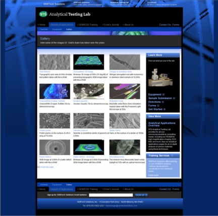
SEMTech Solutions Analytical Testing Laboratory has launched a new website designed to showcase its capabilities through a gallery of their microscopy work.
“Calling all Microscopists!” SEMTech Solutions new Microscopy Services Website is fast becoming a reference library for materials analysis.
North Billerica, MA | Posted on April 29th, 2009SEMTech Solutions Analytical Testing Laboratory announces the launch of its new website. The site can be found at www.atl.semtechsolutions.com.
This new website provides users with images and descriptions of Scanning Electron Microscopy (SEM) techniques for various materials. Also included is information about SEMTech Solution's services, capabilities, and equipment. Visitors to the site will be able to access on-line instructions and forms to submit samples for testing and analysis.
"We are excited to launch the new website and view this as an opportunity to provide our current and potential partners with detailed information regarding our capabilities," said Dr. Ernie Dobi, Lab Manager. "Furthermore, the new website will allow users to readily get the information they need when selecting our FE-SEM Analytical Testing Laboratory as their laboratory of choice."
####
About SEMTech Solutions, Inc
SEMTech Solutions Microscopy Laboratory is located in North Billerica, Massachusetts USA. Our Microscopy Lab is an unbiased resource, providing confidential research and developmental support for materials testing, identification, technical problem solving, and analysis. Our laboratory includes a Field Emission Scanning Electron Microscope (FE-SEM), a unique 3D FE-SEM for surface roughness analysis, a Polarizing Light Microscope (PLM), and several stereo optical microscopes. The FE-SEM is also equipped with a Silicon Drift Elemental Dispersive Spectrometer (EDS) for elemental analysis and Robinson Backscattered Electron (BSE) Detector for atomic number imaging.
For more information, please click here
Contacts:
Marketing Contact:
Gary Brake
(978) 663-9822 x232
SEMTech Solutions, Inc.
6 Executive Park Drive
North Billerica, MA 01862
(978) 663-9822
Copyright © SEMTech Solutions
If you have a comment, please Contact us.Issuers of news releases, not 7th Wave, Inc. or Nanotechnology Now, are solely responsible for the accuracy of the content.
Bookmark:


| Related News Press |
News and information
![]() Quantum computer improves AI predictions April 17th, 2026
Quantum computer improves AI predictions April 17th, 2026
![]() Flexible sensor gains sensitivity under pressure April 17th, 2026
Flexible sensor gains sensitivity under pressure April 17th, 2026
![]() A reusable chip for particulate matter sensing April 17th, 2026
A reusable chip for particulate matter sensing April 17th, 2026
![]() Detecting vibrational quantum beating in the predissociation dynamics of SF6 using time-resolved photoelectron spectroscopy April 17th, 2026
Detecting vibrational quantum beating in the predissociation dynamics of SF6 using time-resolved photoelectron spectroscopy April 17th, 2026
Imaging
![]() Simple algorithm paired with standard imaging tool could predict failure in lithium metal batteries August 8th, 2025
Simple algorithm paired with standard imaging tool could predict failure in lithium metal batteries August 8th, 2025
Announcements
![]() A fundamentally new therapeutic approach to cystic fibrosis: Nanobody repairs cellular defect April 17th, 2026
A fundamentally new therapeutic approach to cystic fibrosis: Nanobody repairs cellular defect April 17th, 2026
![]() UC Irvine physicists discover method to reverse ‘quantum scrambling’ : The work addresses the problem of information loss in quantum computing system April 17th, 2026
UC Irvine physicists discover method to reverse ‘quantum scrambling’ : The work addresses the problem of information loss in quantum computing system April 17th, 2026
Tools
![]() Metasurfaces smooth light to boost magnetic sensing precision January 30th, 2026
Metasurfaces smooth light to boost magnetic sensing precision January 30th, 2026
![]() From sensors to smart systems: the rise of AI-driven photonic noses January 30th, 2026
From sensors to smart systems: the rise of AI-driven photonic noses January 30th, 2026
![]() Japan launches fully domestically produced quantum computer: Expo visitors to experience quantum computing firsthand August 8th, 2025
Japan launches fully domestically produced quantum computer: Expo visitors to experience quantum computing firsthand August 8th, 2025
|
|
||
|
|
||
| The latest news from around the world, FREE | ||
|
|
||
|
|
||
| Premium Products | ||
|
|
||
|
Only the news you want to read!
Learn More |
||
|
|
||
|
Full-service, expert consulting
Learn More |
||
|
|
||