Home > Press > Catching the lightwave: Nano-mechanical sensors 'wired' by photonics
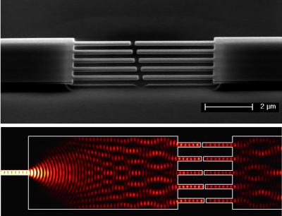 |
| This image shows the electronmicroscopic image of array (top) and simulation of lightwaves through array (bottom).
Credit: Li, Pernice,Tang / Yale |
Abstract:
As researchers push towards detection of single molecules, single electron spins and the smallest amounts of mass and movement, Yale researchers have demonstrated silicon-based nanocantilevers, smaller than the wavelength of light, that operate on photonic principles eliminating the need for electric transducers and expensive laser setups.
Catching the lightwave: Nano-mechanical sensors 'wired' by photonics
New Haven, CT | Posted on April 27th, 2009The work reported in an April 26 advance online publication of Nature Nanotechnology ushers in a new generation of tools for ultra-sensitive measurements at the atomic level.
In nanoelectromechanical systems (NEMS), cantilevers are the most fundamental mechanical sensors. These tiny structures � fixed at one end and free at the other � act like nano-scale diving boards that "bend" when molecules "jump" on them and register a change that can be measured and calibrated. This paper demonstrates how NEMS can be improved by using integrated photonics to sense the cantilever motion.
"The system we developed is the most sensitive available that works at room temperature. Previously this level of sensitivity could only be achieved at extreme low temperatures" said senior author Hong Tang, assistant professor of electrical and mechanical engineering in the Yale School of Engineering and Applied Sciences.
Their system can detect as little deflection in the nano-cantilever sensors as 0.0001 Angstroms � one ten thousandth of the size of an atom
To detect this tiny motion, the Yale team devised a photonic structure to guide the light wave through a cantilever. After exiting from the free end of the cantilever, the light tunnels through a nanometer gap and is collected on chip. "Detecting the lightwave after this evanescent tunneling," says Tang, "gives the unprecedented sensitivity."
Tang's paper also details the construction of a sensor multiplex � a parallel array of 10 nano-cantilevers integrated on a single photonic wire. Each cantilever is a different length, like a key on a xylophone, so when one is displaced it registers its own distinctive "tone."
"A multiplex format lets us make more complex measurements of patterns simultaneously � like a tune with chords instead of single notes," said postdoctoral fellow Mo Li, the lead author of the paper.
At the heart of this breakthrough is the novel way Tang's group "wired" the sensors with light. Their technique is not limited by the bandwidth constraints of electrical methods or the diffraction limits of light sources.
"We don't need a laser to operate these devices," said Wolfram Pernice, a co-author of the paper. "Very cheap LEDs will suffice." Futhermore, the LED light sources � like the million LED pixels that make up a laptop computer screen � can be scaled in size to integrate into a nanophotonic-chip � an important feature for this application.
"This development reinforces the practicality of the new field of nanooptomechanics," says Tang, "and points to a future of compact, robust and scalable systems with high sensitivity that will find a wide range of future applications � from chemical and biological sensing to optical signal processing."
Funding for the research was from a Yale Institute for Nanoscience and Quantum Engineering seed grant, a National Science Foundation career award, and the Alexander-von-Humboldt postdoctoral fellowship programs.
Citation: Nature Nanotechnology: Advance Online Publication April 26, 2009
doi = 10.1038/NNANO.2009.92
####
For more information, please click here
Contacts:
Janet Rettig Emanuel
203-432-2157
Wolfram Pernice
Copyright © Yale University
If you have a comment, please Contact us.Issuers of news releases, not 7th Wave, Inc. or Nanotechnology Now, are solely responsible for the accuracy of the content.
Bookmark:


| Related Links |
![]() Yale School of Engineering and Applied Sciences
Yale School of Engineering and Applied Sciences
![]() Yale Institute for Nanoscience and Quantum Engineering
Yale Institute for Nanoscience and Quantum Engineering
| Related News Press |
News and information
![]() Quantum computer improves AI predictions April 17th, 2026
Quantum computer improves AI predictions April 17th, 2026
![]() Flexible sensor gains sensitivity under pressure April 17th, 2026
Flexible sensor gains sensitivity under pressure April 17th, 2026
![]() A reusable chip for particulate matter sensing April 17th, 2026
A reusable chip for particulate matter sensing April 17th, 2026
![]() Detecting vibrational quantum beating in the predissociation dynamics of SF6 using time-resolved photoelectron spectroscopy April 17th, 2026
Detecting vibrational quantum beating in the predissociation dynamics of SF6 using time-resolved photoelectron spectroscopy April 17th, 2026
Govt.-Legislation/Regulation/Funding/Policy
![]() Quantum computer improves AI predictions April 17th, 2026
Quantum computer improves AI predictions April 17th, 2026
![]() Metasurfaces smooth light to boost magnetic sensing precision January 30th, 2026
Metasurfaces smooth light to boost magnetic sensing precision January 30th, 2026
![]() New imaging approach transforms study of bacterial biofilms August 8th, 2025
New imaging approach transforms study of bacterial biofilms August 8th, 2025
Discoveries
![]() Quantum computer improves AI predictions April 17th, 2026
Quantum computer improves AI predictions April 17th, 2026
![]() Flexible sensor gains sensitivity under pressure April 17th, 2026
Flexible sensor gains sensitivity under pressure April 17th, 2026
![]() A reusable chip for particulate matter sensing April 17th, 2026
A reusable chip for particulate matter sensing April 17th, 2026
![]() Detecting vibrational quantum beating in the predissociation dynamics of SF6 using time-resolved photoelectron spectroscopy April 17th, 2026
Detecting vibrational quantum beating in the predissociation dynamics of SF6 using time-resolved photoelectron spectroscopy April 17th, 2026
Announcements
![]() A fundamentally new therapeutic approach to cystic fibrosis: Nanobody repairs cellular defect April 17th, 2026
A fundamentally new therapeutic approach to cystic fibrosis: Nanobody repairs cellular defect April 17th, 2026
![]() UC Irvine physicists discover method to reverse �quantum scrambling� : The work addresses the problem of information loss in quantum computing system April 17th, 2026
UC Irvine physicists discover method to reverse �quantum scrambling� : The work addresses the problem of information loss in quantum computing system April 17th, 2026
Photonics/Optics/Lasers
![]() Metasurfaces smooth light to boost magnetic sensing precision January 30th, 2026
Metasurfaces smooth light to boost magnetic sensing precision January 30th, 2026
![]() From sensors to smart systems: the rise of AI-driven photonic noses January 30th, 2026
From sensors to smart systems: the rise of AI-driven photonic noses January 30th, 2026
|
|
||
|
|
||
| The latest news from around the world, FREE | ||
|
|
||
|
|
||
| Premium Products | ||
|
|
||
|
Only the news you want to read!
Learn More |
||
|
|
||
|
Full-service, expert consulting
Learn More |
||
|
|
||