Home > Press > Bridging the gap in nanoantennas
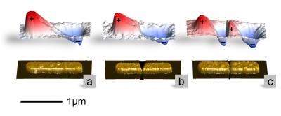 |
| The bottom line depicts the topography, whereas the upper line plots the scanned near-field images. Figure a shows a metal nanorod that can be considered the most simple dipole antenna. The near-field image clearly shows the dipolar oscillation mode with positive fields in red and negative fields in blue color. By introducing a narrow gap at the center of the nanorod thus altering the "antenna load" (Figure c), two dipolar-like modes are obtained. When the gap is connected with a small metal bridge (Figure b), the dipole oscillation mode of Figure a can be restored as the near-field image clearly reveals.
Credit: Martin Schnell/CIC nanoGUNE |
Abstract:
In a recent publication in Nature Photonics, a joint team of researchers at CIC nanoGUNE, Donostia International Physics Center DIPC, Centro de Física de Materiales of CSIC/UPV-EHU in San Sebastian (Spain), Harvard University (USA) and the Max Planck Institute of Biochemistry in Munich (Germany) reports an innovative method for controlling light on the nanoscale by adopting tuning concepts from radio-frequency technology. The method opens the door for targeted design of antenna-based applications including highly sensitive biosensors and extremely fast photodetectors, which could play an important role in future biomedical diagnostics and information processing.
Bridging the gap in nanoantennas
San Sebastian, Spain, Cambridge, MA and Munich, Germany | Posted on April 22nd, 2009An antenna is a device designed to transmit or receive electromagnetic waves. Radio frequency antennas find wide use in systems such as radio and television broadcasting, point-to-point radio communication, wireless LAN, radar, and space exploration. In turn, an optical antenna is a device which acts as an effective receiver and transmitter of visible or infrared light. It has the ability to concentrate (focus) light to tiny spots of nanometer-scale dimensions, which is several orders of magnitude smaller than what conventional lenses can achieve. Tiny objects such as molecules or semiconductors that are placed into these so-called "hot spots" of the antenna can efficiently interact with light. Therefore optical antennas boost single molecule spectroscopy or signal-to-noise in detector applications.
In their experiments the researchers studied a special type of infrared antennas, featuring a very narrow gap at the center. These so called gap-antennas generate a very intense "hot spot" inside the gap, allowing for highly efficient nano-focusing of light. To study how the presence of matter inside the gap (the "load") affects the antenna behavior, the researchers fabricated small metal bridges inside the gap (Figure b). They mapped the near-field oscillations of the different antennas with a modified version of the scattering-type near-field microscope that the Max Planck and nanoGUNE researchers had pioneered over the last decade. For this work, they chose dielectric tips and operated in transmission mode, allowing for imaging local antenna fields in details as small as 50 nm without disturbing the antenna. "By monitoring the near-field oscillations of the different antennas with our novel near-field microscope, we were able to directly visualize how matter inside the gap affects the antenna response. The effect could find interesting applications for tuning of optical antennas" says Rainer Hillenbrand leader of the Nanooptics group at the newly established research institute CIC nanoGUNE Consolider.
The nanooptics group from DIPC and CSIC-UPV/EHU led by Javier Aizpurua in San Sebastián fully confirmed and helped to understand the experimental results by means of full electrodynamic calculations. The calculated maps of the antenna fields are in good agreement with the experimentally observed images. The simulations add deep insights into the dependence of the antenna modes on the bridging, thus confirming the validity and robustness of the "loading" concept to manipulate and control nanoscale local fields in optics.
Furthermore, the researchers applied the well developed radio-frequency antenna design concepts to visible and infrared frequencies, and explained the behavior of the loaded antennas within the framework of optical circuit theory. A simple circuit model showed remarkable agreement with the results of the numerical calculations of the optical resonances. "By extending circuit theory to visible and infrared frequencies, the design of novel photonic devices and detectors will become more efficient. This bridges the gap between these two disciplines" says Javier Aizpurua.
With this work, the researches provide first experimental evidence that the local antenna fields can be controlled by gap-loading. This opens the door for designing near-field patterns in the nanoscale by load manipulation, without the need to change antenna length, which could be highly valuable for the development of compact and integrated nanophotonic devices.
####
For more information, please click here
Contacts:
Oihane Lakar
34-943-363-040
Dr. Rainer Hillenbrand
Nanooptics Laboratory
CIC nanoGUNE Consolider
Tolosa Hiribidea 76
200018 Donostia - San Sebastian, Spain
phone: +34 943 574 007
www.nanogune.eu
Copyright © Elhuyar Fundazioa
If you have a comment, please Contact us.Issuers of news releases, not 7th Wave, Inc. or Nanotechnology Now, are solely responsible for the accuracy of the content.
Bookmark:


| Related News Press |
News and information
![]() Quantum computer improves AI predictions April 17th, 2026
Quantum computer improves AI predictions April 17th, 2026
![]() Flexible sensor gains sensitivity under pressure April 17th, 2026
Flexible sensor gains sensitivity under pressure April 17th, 2026
![]() A reusable chip for particulate matter sensing April 17th, 2026
A reusable chip for particulate matter sensing April 17th, 2026
![]() Detecting vibrational quantum beating in the predissociation dynamics of SF6 using time-resolved photoelectron spectroscopy April 17th, 2026
Detecting vibrational quantum beating in the predissociation dynamics of SF6 using time-resolved photoelectron spectroscopy April 17th, 2026
Nanomedicine
![]() A fundamentally new therapeutic approach to cystic fibrosis: Nanobody repairs cellular defect April 17th, 2026
A fundamentally new therapeutic approach to cystic fibrosis: Nanobody repairs cellular defect April 17th, 2026
![]() New molecular technology targets tumors and simultaneously silences two ‘undruggable’ cancer genes August 8th, 2025
New molecular technology targets tumors and simultaneously silences two ‘undruggable’ cancer genes August 8th, 2025
![]() New imaging approach transforms study of bacterial biofilms August 8th, 2025
New imaging approach transforms study of bacterial biofilms August 8th, 2025
![]() Electrifying results shed light on graphene foam as a potential material for lab grown cartilage June 6th, 2025
Electrifying results shed light on graphene foam as a potential material for lab grown cartilage June 6th, 2025
Sensors
![]() Flexible sensor gains sensitivity under pressure April 17th, 2026
Flexible sensor gains sensitivity under pressure April 17th, 2026
![]() Tiny nanosheets, big leap: A new sensor detects ethanol at ultra-low levels January 30th, 2026
Tiny nanosheets, big leap: A new sensor detects ethanol at ultra-low levels January 30th, 2026
![]() From sensors to smart systems: the rise of AI-driven photonic noses January 30th, 2026
From sensors to smart systems: the rise of AI-driven photonic noses January 30th, 2026
![]() Sensors innovations for smart lithium-based batteries: advancements, opportunities, and potential challenges August 8th, 2025
Sensors innovations for smart lithium-based batteries: advancements, opportunities, and potential challenges August 8th, 2025
Discoveries
![]() Quantum computer improves AI predictions April 17th, 2026
Quantum computer improves AI predictions April 17th, 2026
![]() Flexible sensor gains sensitivity under pressure April 17th, 2026
Flexible sensor gains sensitivity under pressure April 17th, 2026
![]() A reusable chip for particulate matter sensing April 17th, 2026
A reusable chip for particulate matter sensing April 17th, 2026
![]() Detecting vibrational quantum beating in the predissociation dynamics of SF6 using time-resolved photoelectron spectroscopy April 17th, 2026
Detecting vibrational quantum beating in the predissociation dynamics of SF6 using time-resolved photoelectron spectroscopy April 17th, 2026
Announcements
![]() A fundamentally new therapeutic approach to cystic fibrosis: Nanobody repairs cellular defect April 17th, 2026
A fundamentally new therapeutic approach to cystic fibrosis: Nanobody repairs cellular defect April 17th, 2026
![]() UC Irvine physicists discover method to reverse ‘quantum scrambling’ : The work addresses the problem of information loss in quantum computing system April 17th, 2026
UC Irvine physicists discover method to reverse ‘quantum scrambling’ : The work addresses the problem of information loss in quantum computing system April 17th, 2026
|
|
||
|
|
||
| The latest news from around the world, FREE | ||
|
|
||
|
|
||
| Premium Products | ||
|
|
||
|
Only the news you want to read!
Learn More |
||
|
|
||
|
Full-service, expert consulting
Learn More |
||
|
|
||