Home > Press > Breakthrough Nanoindentation Testing With Image Pattern Recognition
 |
Abstract:
Nanovea announced today a breakthrough development in Nanoindentation testing by combining advanced image pattern recognition capabilities to the most advanced nano-indenter for quality control applications.
Breakthrough Nanoindentation Testing With Image Pattern Recognition
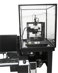
Irvine, CA | Posted on April 15th, 2009Nanovea has now combined their, PRVision, machine vision camera option to Nanoindentation testing that allows auto-recognition of precisely chosen features with little to no user interaction. The user-friendly software of Nanovea's PRVision allows for an automatic test of hardness and elastic modulus on patterned samples or specifically chosen areas of interest. Nanoindentation properties including hardness and elastic modulus can then be automatically measured and recorded. The "quasi non-destructive" low loads associated with Nanoindentation Testing makes this technique an ideal breakthrough tool to monitor the quality control of environments where hardness and elastic modulus are crucial: Micro Electronics, Solar, Pharmaceuticals and many others.
"Nanoindentation until now was performed using primitive mapping options. Our PRVision option will speed up Nanoindentation testing and opens the door to wide-scale automatic production quality control applications where hardness and elastic modulus are the best control parameters." Said Pierre Leroux, CEO/President, Nanovea.
####
About Nanovea
Nanovea is the result of 16 years that Micro Photonics Inc. has provided professional solutions and experienced service throughout the profilometry, nano/micro/macro mechanical, tribology, micro tomography, imaging and other related fields of materials and thin films research and development industries. After years of client feedback and the dedication to providing superior instrumental solutions Nanovea was launched in 2004 at the Micro Photonics Inc. office in Irvine CA.
For more information, please click here
Contacts:
Ray Weedman
NANOVEA
949.461.9292
Copyright © PRWeb�
If you have a comment, please Contact us.Issuers of news releases, not 7th Wave, Inc. or Nanotechnology Now, are solely responsible for the accuracy of the content.
Bookmark:


| Related News Press |
News and information
![]() Quantum computer improves AI predictions April 17th, 2026
Quantum computer improves AI predictions April 17th, 2026
![]() Flexible sensor gains sensitivity under pressure April 17th, 2026
Flexible sensor gains sensitivity under pressure April 17th, 2026
![]() A reusable chip for particulate matter sensing April 17th, 2026
A reusable chip for particulate matter sensing April 17th, 2026
![]() Detecting vibrational quantum beating in the predissociation dynamics of SF6 using time-resolved photoelectron spectroscopy April 17th, 2026
Detecting vibrational quantum beating in the predissociation dynamics of SF6 using time-resolved photoelectron spectroscopy April 17th, 2026
Announcements
![]() A fundamentally new therapeutic approach to cystic fibrosis: Nanobody repairs cellular defect April 17th, 2026
A fundamentally new therapeutic approach to cystic fibrosis: Nanobody repairs cellular defect April 17th, 2026
![]() UC Irvine physicists discover method to reverse �quantum scrambling� : The work addresses the problem of information loss in quantum computing system April 17th, 2026
UC Irvine physicists discover method to reverse �quantum scrambling� : The work addresses the problem of information loss in quantum computing system April 17th, 2026
Tools
![]() Metasurfaces smooth light to boost magnetic sensing precision January 30th, 2026
Metasurfaces smooth light to boost magnetic sensing precision January 30th, 2026
![]() From sensors to smart systems: the rise of AI-driven photonic noses January 30th, 2026
From sensors to smart systems: the rise of AI-driven photonic noses January 30th, 2026
![]() Japan launches fully domestically produced quantum computer: Expo visitors to experience quantum computing firsthand August 8th, 2025
Japan launches fully domestically produced quantum computer: Expo visitors to experience quantum computing firsthand August 8th, 2025
|
|
||
|
|
||
| The latest news from around the world, FREE | ||
|
|
||
|
|
||
| Premium Products | ||
|
|
||
|
Only the news you want to read!
Learn More |
||
|
|
||
|
Full-service, expert consulting
Learn More |
||
|
|
||