Home > Press > New way to produce electronic components can lead to cheap and flexible electronics
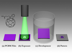 |
| En PCBM-fullerenfilm mĺlas ut pĺ ett substrat. (b) Valda delar av filmen exponeras med laserljus (här via användande av en svart skuggmask). (c) Hela filmen framkallas genom att doppas i en framkallningsvätska. (d) Ett elektroniskt aktivt PCBM-mönster framträder där laserljuset träffat. |
Abstract:
Flexible display screens and cheap solar cells can become a reality through research and development in organic electronics. Physicists at Umeĺ University in Sweden have now developed a new and simple method for producing cheap electronic components.
New way to produce electronic components can lead to cheap and flexible electronics
Umeĺ, Sweden | Posted on March 26th, 2009"The method is simple and can therefore be of interest for future mass production of cheap electronics," says physicist Ludvig Edman.
Organic chemistry is a rapidly expanding research field that promises exciting and important applications such as flexible display screens and cheap solar cells. One attractive feature is that organic electronic materials can be processed from a solution.
"This makes it possible to paint thin films of electronic materials on flexible surfaces like paper or plastic," explains Ludvig Edman.
Electronic components with various functions can then be created by patterning the film with a specific structure. Until now it has proven to be problematic to carry out this patterning in a simple way without destroying the electronic properties of the organic material.
"We have now developed a method that enables us to create patterns in an efficient and gentle way. With the patterned organic material as a base, we have managed to produce well-functioning transistors," says Ludvig Edman.
A thin film of an organic electronic material, a so-called fullerene, is first painted on a selected surface. The parts of the film that are to remain in place are directly exposed to laser light. Then the whole film can be developed by rinsing it with a solution. A well-defined pattern then emerges where the laser light hit the surface.
A key advantage with this method of patterning is that it is both simple and scalable, which means that it can be useful in future production of cheap and flexible electronics in an assembly line process.
Other researchers involved in developing the method are Andrzej Dzwilewski and Thomas Wĺgberg.
The findings are presented in the industry publication Journal of the American Chemical Society (2009, 131, 4006-4011).
####
About Umeĺ University
Umeĺ University was founded in 1965 and is Sweden's fifth oldest university. Today, we have a strong international and multicultural presence with students, teachers and researchers from all over the world. Our main campus - with its 29,000 students and 4,000 employees - is alive with enthusiasm, creativity and fresh ideas.
We constantly strive towards making it one of Scandinavia's best environments for study and research that meets the challenges of an ever-increasing global society.
Contacts:
Ludvig Edman
Senior Lecturer of Physics
Phone: +46 (0)90-786 57 32
Mobile: +46 (0)70-232 12 40
Copyright © Umeĺ University
If you have a comment, please Contact us.Issuers of news releases, not 7th Wave, Inc. or Nanotechnology Now, are solely responsible for the accuracy of the content.
Bookmark:


| Related News Press |
News and information
![]() Quantum computer improves AI predictions April 17th, 2026
Quantum computer improves AI predictions April 17th, 2026
![]() Flexible sensor gains sensitivity under pressure April 17th, 2026
Flexible sensor gains sensitivity under pressure April 17th, 2026
![]() A reusable chip for particulate matter sensing April 17th, 2026
A reusable chip for particulate matter sensing April 17th, 2026
![]() Detecting vibrational quantum beating in the predissociation dynamics of SF6 using time-resolved photoelectron spectroscopy April 17th, 2026
Detecting vibrational quantum beating in the predissociation dynamics of SF6 using time-resolved photoelectron spectroscopy April 17th, 2026
Thin films
![]() Tiny nanosheets, big leap: A new sensor detects ethanol at ultra-low levels January 30th, 2026
Tiny nanosheets, big leap: A new sensor detects ethanol at ultra-low levels January 30th, 2026
![]() Utilizing palladium for addressing contact issues of buried oxide thin film transistors April 5th, 2024
Utilizing palladium for addressing contact issues of buried oxide thin film transistors April 5th, 2024
![]() Understanding the mechanism of non-uniform formation of diamond film on tools: Paving the way to a dry process with less environmental impact March 24th, 2023
Understanding the mechanism of non-uniform formation of diamond film on tools: Paving the way to a dry process with less environmental impact March 24th, 2023
![]() New study introduces the best graphite films: The work by Distinguished Professor Feng Ding at UNIST has been published in the October 2022 issue of Nature Nanotechnology November 4th, 2022
New study introduces the best graphite films: The work by Distinguished Professor Feng Ding at UNIST has been published in the October 2022 issue of Nature Nanotechnology November 4th, 2022
Announcements
![]() A fundamentally new therapeutic approach to cystic fibrosis: Nanobody repairs cellular defect April 17th, 2026
A fundamentally new therapeutic approach to cystic fibrosis: Nanobody repairs cellular defect April 17th, 2026
![]() UC Irvine physicists discover method to reverse ‘quantum scrambling’ : The work addresses the problem of information loss in quantum computing system April 17th, 2026
UC Irvine physicists discover method to reverse ‘quantum scrambling’ : The work addresses the problem of information loss in quantum computing system April 17th, 2026
Solar/Photovoltaic
![]() Spinel-type sulfide semiconductors to operate the next-generation LEDs and solar cells For solar-cell absorbers and green-LED source October 3rd, 2025
Spinel-type sulfide semiconductors to operate the next-generation LEDs and solar cells For solar-cell absorbers and green-LED source October 3rd, 2025
![]() KAIST researchers introduce new and improved, next-generation perovskite solar cell November 8th, 2024
KAIST researchers introduce new and improved, next-generation perovskite solar cell November 8th, 2024
![]() Groundbreaking precision in single-molecule optoelectronics August 16th, 2024
Groundbreaking precision in single-molecule optoelectronics August 16th, 2024
![]() Development of zinc oxide nanopagoda array photoelectrode: photoelectrochemical water-splitting hydrogen production January 12th, 2024
Development of zinc oxide nanopagoda array photoelectrode: photoelectrochemical water-splitting hydrogen production January 12th, 2024
|
|
||
|
|
||
| The latest news from around the world, FREE | ||
|
|
||
|
|
||
| Premium Products | ||
|
|
||
|
Only the news you want to read!
Learn More |
||
|
|
||
|
Full-service, expert consulting
Learn More |
||
|
|
||