Home > Press > Filmetrics Launches Thin-film Photovoltaic Dedicated Metrology Systems
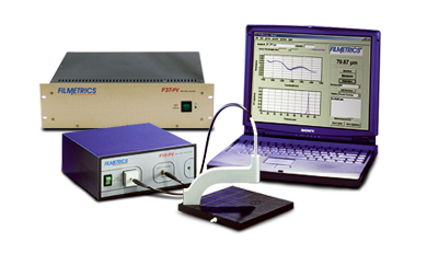 |
| F10-PV and F37-PV are commercially available thin-film metrology solutions capable of measuring all classes of films used in today's TFPV industry |
Abstract:
High-speed, reliable, and affordable metrology solutions for every class of thin-film photovoltaic material used in today's industry
Filmetrics Launches Thin-film Photovoltaic Dedicated Metrology Systems
San Diego, CA | Posted on March 19th, 2009Filmetrics announces the launch of its thin-film photovoltaic (TFPV) dedicated measurement systems. With the release of the F10-PV and the F37-PV Filmetrics now offers commercially available tabletop and in-line metrology solutions for industries utilizing all classes of TFPV materials. Typically built on or under transparent conductive oxides (TCO) on glass, plastics, or metal substrates, the properties of TFPV films are notoriously difficult to measure due to their special optical properties. Filmetrics has SOLVED this problem for all classes of films used in today's industry.
The Filmetrics F10-PV and F37-PV products are capable of monitoring the film thickness of active layers such as amorphous Si, CdS, CdTe, copper-indium gallium diselenide (CIGS), TCOs, and buffer layers. These types of devices are intentionally designed to absorb rather than reflect light creating many unique challenges for performing metrology on these layers. Surmounting these challenges the F10-PV and the F37-PV can accurately measure the thickness and optical properties of even the most complex structures on TCOs adding unrivalled value in terms of production quality, efficiency, and cost control for TFPV device manufacturers.
Strong market demand, and working closely with our existing TFPV customer base, led Filmetrics to undergo extensive collaborative research in the past months to develop these products. The addition of non-destructive thin-film thickness metrology to the TFPV environment is expected to greatly enhance production efficiency and yields, help develop new processes, and facilitate rapid transfer these new ideas to the production floor.
With years of experience in the thin-film measurement field, Filmetrics provides a simple-to-understand user interface and unparalleled support. Headquartered in San Diego, CA, Filmetrics has a full line of thin-film measurement systems and is continually developing new products and technologies that bring greater efficiency to thin-film metrology. Filmetrics was founded in 1995 and has quickly established itself as the foremost innovator in the thin-film measurement industry.
####
About Filmetrics
Filmetrics, Inc. was founded in 1995 with the mission of making thin-film measurements simple and affordable. Prior to our arrival, commercial thin-film measurement instruments cost $50,000 or more and required operators to have advanced training. Single measurements took several minutes, even hours.
The Filmetrics approach was to design an affordable purpose-built miniature spectrometer system, whose low cost had just recently been made possible by advances in silicon detector array technology. We combined this with sophisticated software that integrated advanced thin-film expertise into a simple, intuitive Windows interface. The result was the F20, a compact system with astounding speed and accuracy, which line operators could be trained to use in a matter of minutes - all at a mere fraction of the cost of traditional instruments.
Our accomplishments have been widely recognized by the industry press, including recognition as one of the "100 Most Technologically Significant" products of the year and one of the "25 Best New Products" of the year.
Contacts:
Scott Chalmers
Filmetrics
(858) 573-9300
Copyright © Filmetrics
If you have a comment, please Contact us.Issuers of news releases, not 7th Wave, Inc. or Nanotechnology Now, are solely responsible for the accuracy of the content.
Bookmark:


| Related Links |
| Related News Press |
News and information
![]() Quantum computer improves AI predictions April 17th, 2026
Quantum computer improves AI predictions April 17th, 2026
![]() Flexible sensor gains sensitivity under pressure April 17th, 2026
Flexible sensor gains sensitivity under pressure April 17th, 2026
![]() A reusable chip for particulate matter sensing April 17th, 2026
A reusable chip for particulate matter sensing April 17th, 2026
![]() Detecting vibrational quantum beating in the predissociation dynamics of SF6 using time-resolved photoelectron spectroscopy April 17th, 2026
Detecting vibrational quantum beating in the predissociation dynamics of SF6 using time-resolved photoelectron spectroscopy April 17th, 2026
Thin films
![]() Tiny nanosheets, big leap: A new sensor detects ethanol at ultra-low levels January 30th, 2026
Tiny nanosheets, big leap: A new sensor detects ethanol at ultra-low levels January 30th, 2026
![]() Utilizing palladium for addressing contact issues of buried oxide thin film transistors April 5th, 2024
Utilizing palladium for addressing contact issues of buried oxide thin film transistors April 5th, 2024
![]() Understanding the mechanism of non-uniform formation of diamond film on tools: Paving the way to a dry process with less environmental impact March 24th, 2023
Understanding the mechanism of non-uniform formation of diamond film on tools: Paving the way to a dry process with less environmental impact March 24th, 2023
![]() New study introduces the best graphite films: The work by Distinguished Professor Feng Ding at UNIST has been published in the October 2022 issue of Nature Nanotechnology November 4th, 2022
New study introduces the best graphite films: The work by Distinguished Professor Feng Ding at UNIST has been published in the October 2022 issue of Nature Nanotechnology November 4th, 2022
Products
![]() Spectradyne Partners with Particle Technology Labs for Measurement Services December 6th, 2018
Spectradyne Partners with Particle Technology Labs for Measurement Services December 6th, 2018
![]() Mode-Changing MEMS Accelerometer from STMicroelectronics Combines High Measurement Resolution and Ultra-Low Power for Industrial Applications November 7th, 2018
Mode-Changing MEMS Accelerometer from STMicroelectronics Combines High Measurement Resolution and Ultra-Low Power for Industrial Applications November 7th, 2018
![]() Fat-Repellent Nanolayers Can Make Oven Cleaning Easier October 17th, 2018
Fat-Repellent Nanolayers Can Make Oven Cleaning Easier October 17th, 2018
![]() Aculon, Inc. Enters into Strategic Partnership Agreement with Henkel Corporation to Supply Key Mobile Device Manufacturers with NanoProof� PCB Waterproof Technology October 17th, 2018
Aculon, Inc. Enters into Strategic Partnership Agreement with Henkel Corporation to Supply Key Mobile Device Manufacturers with NanoProof� PCB Waterproof Technology October 17th, 2018
Announcements
![]() A fundamentally new therapeutic approach to cystic fibrosis: Nanobody repairs cellular defect April 17th, 2026
A fundamentally new therapeutic approach to cystic fibrosis: Nanobody repairs cellular defect April 17th, 2026
![]() UC Irvine physicists discover method to reverse �quantum scrambling� : The work addresses the problem of information loss in quantum computing system April 17th, 2026
UC Irvine physicists discover method to reverse �quantum scrambling� : The work addresses the problem of information loss in quantum computing system April 17th, 2026
Tools
![]() Metasurfaces smooth light to boost magnetic sensing precision January 30th, 2026
Metasurfaces smooth light to boost magnetic sensing precision January 30th, 2026
![]() From sensors to smart systems: the rise of AI-driven photonic noses January 30th, 2026
From sensors to smart systems: the rise of AI-driven photonic noses January 30th, 2026
![]() Japan launches fully domestically produced quantum computer: Expo visitors to experience quantum computing firsthand August 8th, 2025
Japan launches fully domestically produced quantum computer: Expo visitors to experience quantum computing firsthand August 8th, 2025
|
|
||
|
|
||
| The latest news from around the world, FREE | ||
|
|
||
|
|
||
| Premium Products | ||
|
|
||
|
Only the news you want to read!
Learn More |
||
|
|
||
|
Full-service, expert consulting
Learn More |
||
|
|
||