Home > Press > Agilent Technologies Expands Capabilities of Highly Versatile: Atomic Force Microscope for Large and Small Samples
 |
Abstract:
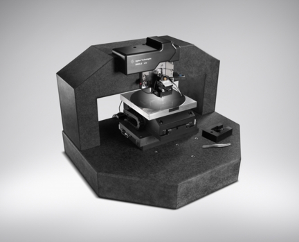
Agilent Technologies Inc. (NYSE: A) today announced the addition of several new capabilities to the Agilent 5600LS, a high-resolution atomic force microscope that utilizes a fully addressable 200mm x 200mm stage and a low-noise AFM design to image both large and small samples. For ultimate flexibility, the 5600LS stage can now accommodate either a single large sample or multiple small samples, each of whose locations can be programmed into the state-of-the-art AFM system. Outstanding instrument versatility makes the 5600LS an ideal choice for multi-user facilities.
Agilent Technologies Expands Capabilities of Highly Versatile: Atomic Force Microscope for Large and Small Samples
Chandler, AZ | Posted on March 11th, 2009 "The 5600LS is the world's only commercially available AFM that allows imaging of large samples in air as well as small samples either in air or in liquid under temperature control with a high-resolution 9-micron scanner," said Jeff Jones, operations manager for Agilent's AFM facility in Chandler, Arizona. "The 5600LS system's ability to utilize open- and closed-loop scanners with a 9-micron scan range allows imaging of small feature sets at atomic resolution. This advanced multipurpose AFM enables a remarkably broad set of nanotechnology applications, including semiconductor, materials science, and life science studies."
A special Agilent stage adapter permits the 5600LS to be used with a sample plate that facilitates in-fluid imaging of small samples. Heating and cooling control is also offered for imaging biological and polymer samples in liquid. Agilent's patented MAC Mode gives 5600LS users industry-leading performance for in-fluid and soft-sample imaging.
The 5600LS supports all major AFM modes. Utilization of MAC Mode III provides three user-configurable lock-in amplifiers, affording researchers virtually limitless application possibilities and unprecedented speed. MAC Mode III allows single-pass imaging concurrent with KFM/EFM, facilitates vertical or lateral modulation studies, and supports the use of higher resonance modes of the cantilever.
The 5600LS is also compatible with Agilent's unique scanning microwave microscopy (SMM) mode, which combines the compound, calibrated electrical measurement capabilities of a microwave vector network analyzer (VNA) with the nanoscale spatial resolution and high-precision positioning of an atomic force microscope for the first time. SMM Mode outperforms traditional AFM-based scanning capacitance microscopy techniques, offering far greater application versatility, the ability to acquire quantitative results, and the highest sensitivity and dynamic range in the industry.
AFM Instrumentation from Agilent Technologies
Agilent Technologies offers high-precision, modular AFM solutions for research, industry, and education. Exceptional worldwide support is provided by experienced application scientists and technical service personnel. Agilent's leading-edge R&D laboratories ensure the continued, timely introduction and optimization of innovative, easy-to-use AFM technologies.
####
About Agilent Technologies Inc.
Agilent Technologies Inc. (NYSE: A) is the world�s premier measurement company and a technology leader in communications, electronics, life sciences, and chemical analysis. The company�s 19,000 employees serve customers in more than 110 countries. Agilent had net revenues of $5.4 billion in fiscal 2007.
For more information, please click here
Contacts:
Joan Horwitz
+1 480 756 5905
Copyright © Agilent Technologies Inc.
If you have a comment, please Contact us.Issuers of news releases, not 7th Wave, Inc. or Nanotechnology Now, are solely responsible for the accuracy of the content.
Bookmark:


| Related News Press |
News and information
![]() Quantum computer improves AI predictions April 17th, 2026
Quantum computer improves AI predictions April 17th, 2026
![]() Flexible sensor gains sensitivity under pressure April 17th, 2026
Flexible sensor gains sensitivity under pressure April 17th, 2026
![]() A reusable chip for particulate matter sensing April 17th, 2026
A reusable chip for particulate matter sensing April 17th, 2026
![]() Detecting vibrational quantum beating in the predissociation dynamics of SF6 using time-resolved photoelectron spectroscopy April 17th, 2026
Detecting vibrational quantum beating in the predissociation dynamics of SF6 using time-resolved photoelectron spectroscopy April 17th, 2026
Imaging
![]() Simple algorithm paired with standard imaging tool could predict failure in lithium metal batteries August 8th, 2025
Simple algorithm paired with standard imaging tool could predict failure in lithium metal batteries August 8th, 2025
Announcements
![]() A fundamentally new therapeutic approach to cystic fibrosis: Nanobody repairs cellular defect April 17th, 2026
A fundamentally new therapeutic approach to cystic fibrosis: Nanobody repairs cellular defect April 17th, 2026
![]() UC Irvine physicists discover method to reverse �quantum scrambling� : The work addresses the problem of information loss in quantum computing system April 17th, 2026
UC Irvine physicists discover method to reverse �quantum scrambling� : The work addresses the problem of information loss in quantum computing system April 17th, 2026
Tools
![]() Metasurfaces smooth light to boost magnetic sensing precision January 30th, 2026
Metasurfaces smooth light to boost magnetic sensing precision January 30th, 2026
![]() From sensors to smart systems: the rise of AI-driven photonic noses January 30th, 2026
From sensors to smart systems: the rise of AI-driven photonic noses January 30th, 2026
![]() Japan launches fully domestically produced quantum computer: Expo visitors to experience quantum computing firsthand August 8th, 2025
Japan launches fully domestically produced quantum computer: Expo visitors to experience quantum computing firsthand August 8th, 2025
|
|
||
|
|
||
| The latest news from around the world, FREE | ||
|
|
||
|
|
||
| Premium Products | ||
|
|
||
|
Only the news you want to read!
Learn More |
||
|
|
||
|
Full-service, expert consulting
Learn More |
||
|
|
||