Home > Press > New Record for World's Smallest Letters: Stanford University breaks record set in 1991, promises denser information storage
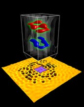 |
| Molecular holograms are fashioned with scanning tunneling microscope manipulation. When illuminated by two-dimensional electron gas, a three-dimensional holographic projection is created.
Here, two pages of information, the red and blue letters, are retrieved from a data cube verifying that the quantum nature of electron states has features smaller than anything possible or that can be used to construct elements such as letters directly with atoms. The information density limit of discrete matter identified with atomic manipulation is surpassed by showing that electrons are capable of subatomic encoding. Credit: Image credit: Hari Manoharan / Stanford University |
Abstract:
A novel technique that enables researchers to push individual molecules into specifically arranged patterns recently allowed researchers at Stanford University to shatter the long held belief that one bit per atom is the limit for encoding information and reclaim the title of producers of the world's smallest letters.
New Record for World's Smallest Letters: Stanford University breaks record set in 1991, promises denser information storage
Arlington, VA | Posted on March 11th, 2009Researchers Hari Manoharan and Christopher Moon along with students at Stanford's Physics Department and Geballe Laboratory for Advanced Materials were able to encode 35 bits of information per electron and write letters so small, they are composed of subatomic bits of size 0.3 nanometers, or roughly one third of a billionth of a meter.
The feat edges out researchers at Japanese firm Hitachi, who in 1991 set the record for microscopic calligraphy by chiseling 1.5-nanometre-tall letters into a certain type of crystal.
Stanford's research is supported by the National Science Foundation, the Department of Energy's SLAC National Accelerator Laboratory, the Stanford Institute for Materials and Energy Science, the Office of Naval Research, and the Stanford-IBM Center for Probing the Nanoscale.
Researchers say the small size of letters could enable information to be stored more densely providing greater speed and storage capacity for modern computers. In fact, the letters formed, an "S" and a "U" for Stanford University, are so small they could be used to print the 32-volume Encyclopedia Britannica 2,000 times and the contents would fit on the head of a pin.
To shrink the letters, Manoharan and Moon used a scanning tunneling microscope to arrange individual carbon monoxide molecules on a copper surface in a complicated two-dimensional pattern engineered with a void in the middle into which they desired to project electronic versions of the letters.
They then used the constant flow of electrons naturally present on the copper surface to form the letters. The electrons, rippling over the surface as waves, scattered off any carbon monoxide molecules they met and worked to project holographic patterns of the letters into the void.
The letters were formed in the void by waves of quantum electrons with very small wavelengths. In this way, the two-dimensional pattern of molecules functioned as a molecular-sized hologram, illuminated with electrons instead of light.
"Imagine the copper as a very shallow pool of water into which we put some rocks [the carbon monoxide molecules]," says Manoharan. "The water waves scatter and interfere off the rocks, making well-defined standing wave patterns." If the rocks are positioned just right, the wave patterns will form into letters.
Called "Electronic Quantum Holography," the process was carried out in a vibration proof basement on Stanford's campus.
"In this experiment we've stored some 35 bits per electron to encode each letter," said Manoharan. "We write the letters so small that the bits that comprise them are subatomic in size. So one bit per atom is no longer the limit for information density. There's a grand new horizon below that, in the subatomic regime. Indeed, there's even more room at the bottom than we ever imagined."
A paper on Manoharan's and Moon's work, "Quantum Holographic Encoding in a Two-Dimensional Electron Gas," was published online in Nature Nanotechnology.
####
About National Science Foundation
The National Science Foundation (NSF) is an independent federal agency that supports fundamental research and education across all fields of science and engineering, with an annual budget of $6.06 billion. NSF funds reach all 50 states through grants to over 1,900 universities and institutions. Each year, NSF receives about 45,000 competitive requests for funding, and makes over 11,500 new funding awards. NSF also awards over $400 million in professional and service contracts yearly.
For more information, please click here
Contacts:
Bobbie Mixon
(703) 292-8485
Copyright © National Science Foundation
If you have a comment, please Contact us.Issuers of news releases, not 7th Wave, Inc. or Nanotechnology Now, are solely responsible for the accuracy of the content.
Bookmark:


| Related News Press |
News and information
![]() Quantum computer improves AI predictions April 17th, 2026
Quantum computer improves AI predictions April 17th, 2026
![]() Flexible sensor gains sensitivity under pressure April 17th, 2026
Flexible sensor gains sensitivity under pressure April 17th, 2026
![]() A reusable chip for particulate matter sensing April 17th, 2026
A reusable chip for particulate matter sensing April 17th, 2026
![]() Detecting vibrational quantum beating in the predissociation dynamics of SF6 using time-resolved photoelectron spectroscopy April 17th, 2026
Detecting vibrational quantum beating in the predissociation dynamics of SF6 using time-resolved photoelectron spectroscopy April 17th, 2026
Chip Technology
![]() A reusable chip for particulate matter sensing April 17th, 2026
A reusable chip for particulate matter sensing April 17th, 2026
![]() Metasurfaces smooth light to boost magnetic sensing precision January 30th, 2026
Metasurfaces smooth light to boost magnetic sensing precision January 30th, 2026
Memory Technology
![]() Researchers tackle the memory bottleneck stalling quantum computing October 3rd, 2025
Researchers tackle the memory bottleneck stalling quantum computing October 3rd, 2025
![]() First real-time observation of two-dimensional melting process: Researchers at Mainz University unveil new insights into magnetic vortex structures August 8th, 2025
First real-time observation of two-dimensional melting process: Researchers at Mainz University unveil new insights into magnetic vortex structures August 8th, 2025
![]() Utilizing palladium for addressing contact issues of buried oxide thin film transistors April 5th, 2024
Utilizing palladium for addressing contact issues of buried oxide thin film transistors April 5th, 2024
Announcements
![]() A fundamentally new therapeutic approach to cystic fibrosis: Nanobody repairs cellular defect April 17th, 2026
A fundamentally new therapeutic approach to cystic fibrosis: Nanobody repairs cellular defect April 17th, 2026
![]() UC Irvine physicists discover method to reverse �quantum scrambling� : The work addresses the problem of information loss in quantum computing system April 17th, 2026
UC Irvine physicists discover method to reverse �quantum scrambling� : The work addresses the problem of information loss in quantum computing system April 17th, 2026
|
|
||
|
|
||
| The latest news from around the world, FREE | ||
|
|
||
|
|
||
| Premium Products | ||
|
|
||
|
Only the news you want to read!
Learn More |
||
|
|
||
|
Full-service, expert consulting
Learn More |
||
|
|
||