Home > Press > Engis Laboratory Offers Bespoke Advanced Materials Expertise
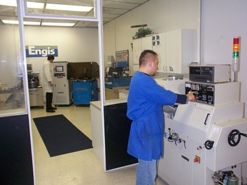 |
| Engis UK laboratory in Henley-on-Thames, UK |
Abstract:
Leading developer of diamond superabrasive finishing systems for the manufacture of MEMS, data storage components, optics and opto-electronics, Engis Corporation has created a network of Advanced Materials Processing Laboratories around the world, first at its Illinois HQ, and now in Japan and the UK, where the Henley-on-Thames facility provides a European resource for developers seeking technical support and expertise in polishing and thinning of advanced materials.
Engis Laboratory Offers Bespoke Advanced Materials Expertise
UK | Posted on March 5th, 2009In these laboratories expert staff work directly with manufacturers and researchers to solve the technical challenges posed by processing the raft of new materials now being used in the production environment. This close collaboration enables new production processes to be developed concurrently with product designs, so delivering highly technical products to the market more quickly and with greater reliability.
The core concept behind the Advanced Materials Laboratories is Engis' integrated approach to diamond superabrasive technology, which brings together all the different components of the process, from machine tools, plates, pads and facing tools equipment to consumables such as slurries and lubricants, into one unified solution, each element of which is under Engis' complete control. Staff in the network of laboratories work together, pooling their expertise to focus on an individual polishing and lapping requirement, providing global expertise at a local level.
The first stage in the development process is to obtain an in-depth understanding of the requirements of each customer, creating a modular process to suit each unique set of requirements, including constraints such as existing equipment, waste management and disposal legislation and/or requirements, speed of throughput and operational cost demands.
Having completely understood the requirements and constraints of the process the unique chemical and mechanical properties of the materials are considered, so that the optimum slurry can be selected, or, if necessary, developed specifically to suit the application, using precisely graded micron diamond which can process extremely hard and chemical resisting materials such as Sapphire, Silicon Carbide, III - V Nitrides and other substrate materials which are frequently used for MEMS and nanotechnology applications.
This level of bespoke development is only possible due to Engis own R&D laboratories and production facilities which enable process engineers to control all the variables including exactly how the diamond is micronized and how the slurry is formulated, the selection and correct charging of the appropriate composite lapping plate and how each production cycle is set up and run.
When all the variables have been examined the whole process is examined in detail once again in order to improve the performance of less expensive earlier steps, to save time and money during more expensive later steps and so create the optimum system of individual process modules, including mounting, machines, slurries and plates, texturing and cleaning.
This laboratory-based solution development provides end-product manufacturers and researchers with real benefits in terms of shorter cycle times, reduced overall consumables costs and shortened CMP process step due to better semi-finishing processes.
It also enables customers to move to "greener", more eco-friendly production processes through a reduced level of consumables and slurry consumption and hence waste disposal and the use of water-soluble easily-cleaned diamond slurries and non-freezing CMP slurries which are less prone to crystallization, while, at the same time maintaining and even enhancing production levels.
Engis MD, John Wellings comments, "Materials such as Gallium Nitride and Silicon Carbide pose specific challenges to developers. Because Engis undertakes extensive R&D activities in its own right, as well as working closely with academic institutions on a range of funded projects, we understand those challenges and are able to assist with leading edge technical expertise."
####
About Engis (UK) Ltd.
Engis (UK) Ltd. is part of the Engis Corporation, a world-wide organisation, established in 1938, which manufactures and markets superabrasive finishing systems for operations that demand precision surface polishing and close tolerance requirements. Engis provides products, services and technological advances in several key areas including: diamond flat lapping/polishing, diamond and CBN-plated tools, bore finishing tools and machines, tool room products and accessories and R&D and technical support.
For more information, please click here
Contacts:
Shelagh Morgan
Tel: 44 01608.663425
Engis (UK) Ltd.
9 Centenary Business Park
Station Road
Henley-on-Thames
Oxon RG9 1DS
Contact: John Wellings
Tel.44 01491.411117
Copyright © Engis (UK) Ltd
If you have a comment, please Contact us.Issuers of news releases, not 7th Wave, Inc. or Nanotechnology Now, are solely responsible for the accuracy of the content.
Bookmark:


| Related News Press |
News and information
![]() Quantum computer improves AI predictions April 17th, 2026
Quantum computer improves AI predictions April 17th, 2026
![]() Flexible sensor gains sensitivity under pressure April 17th, 2026
Flexible sensor gains sensitivity under pressure April 17th, 2026
![]() A reusable chip for particulate matter sensing April 17th, 2026
A reusable chip for particulate matter sensing April 17th, 2026
![]() Detecting vibrational quantum beating in the predissociation dynamics of SF6 using time-resolved photoelectron spectroscopy April 17th, 2026
Detecting vibrational quantum beating in the predissociation dynamics of SF6 using time-resolved photoelectron spectroscopy April 17th, 2026
Laboratories
![]() Researchers develop molecular qubits that communicate at telecom frequencies October 3rd, 2025
Researchers develop molecular qubits that communicate at telecom frequencies October 3rd, 2025
![]() A battery�s hopping ions remember where they�ve been: Seen in atomic detail, the seemingly smooth flow of ions through a battery�s electrolyte is surprisingly complicated February 16th, 2024
A battery�s hopping ions remember where they�ve been: Seen in atomic detail, the seemingly smooth flow of ions through a battery�s electrolyte is surprisingly complicated February 16th, 2024
Materials/Metamaterials/Magnetoresistance
![]() First real-time observation of two-dimensional melting process: Researchers at Mainz University unveil new insights into magnetic vortex structures August 8th, 2025
First real-time observation of two-dimensional melting process: Researchers at Mainz University unveil new insights into magnetic vortex structures August 8th, 2025
![]() Researchers unveil a groundbreaking clay-based solution to capture carbon dioxide and combat climate change June 6th, 2025
Researchers unveil a groundbreaking clay-based solution to capture carbon dioxide and combat climate change June 6th, 2025
![]() A 1960s idea inspires NBI researchers to study hitherto inaccessible quantum states June 6th, 2025
A 1960s idea inspires NBI researchers to study hitherto inaccessible quantum states June 6th, 2025
![]() Institute for Nanoscience hosts annual proposal planning meeting May 16th, 2025
Institute for Nanoscience hosts annual proposal planning meeting May 16th, 2025
Announcements
![]() A fundamentally new therapeutic approach to cystic fibrosis: Nanobody repairs cellular defect April 17th, 2026
A fundamentally new therapeutic approach to cystic fibrosis: Nanobody repairs cellular defect April 17th, 2026
![]() UC Irvine physicists discover method to reverse �quantum scrambling� : The work addresses the problem of information loss in quantum computing system April 17th, 2026
UC Irvine physicists discover method to reverse �quantum scrambling� : The work addresses the problem of information loss in quantum computing system April 17th, 2026
|
|
||
|
|
||
| The latest news from around the world, FREE | ||
|
|
||
|
|
||
| Premium Products | ||
|
|
||
|
Only the news you want to read!
Learn More |
||
|
|
||
|
Full-service, expert consulting
Learn More |
||
|
|
||