Home > Press > SMI offers ZnO Deposition Development Services on 2” through 8” Wafers and Glass Sheets up to 8 “x 8” for: Transparent Contacts (LEDs and Photovoltai
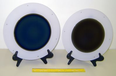 |
| SMI MOCVD grown ZnO thin films (conductive or insulating) through 8” now routinely produced with less than 3% uniformity |
Abstract:
Structured Materials Industries, Inc. (SMI) announces today that it has opened its application lab facilities for the MOCVD growth of ZnO based films for transparent contact work as used with LEDs and photovoltaics, as well as ZnO films for transparent and power transistors.
SMI offers ZnO Deposition Development Services on 2” through 8” Wafers and Glass Sheets up to 8 “x 8” for: Transparent Contacts (LEDs and Photovoltai
Piscataway, NJ | Posted on January 17th, 2009SMI has a decades-long history in development of Zinc Oxide and its alloys and has built considerable capabilities in its in-house applications lab, including 4 ZnO deposition tools, thermal and laser annealing stations, and other support services. These tools are used predominantly in support of customer development needs and deposition tool purchasers.
Our in-house tools include platters are sized at 5" through 12". Materials properties include n-type conductors doped to 10E20 with conductivities as low as ~5E-4 ohm-cm or insulating films at greater than 10E7 ohm-cm. We have experience with a wide range of dopants to tune band gap, index of refraction and conductivity. P-type exploration services are also available.
Our deposition services include demonstrated development of alloys of ZnO (Cd, Mg, Se, Te, and S), doping of ZnO (In, Ga, Al, B, N, P, As, Li, Na, K, and Sb among others) and phosphor or spin materials compositions (Cu, Fe, Co, Mn, Si, Ge, Er, Nb, Eu, and Tb, among others).
Application areas include GaN LEDs, especially UV LEDs, where only ZnO alloys will effectively allow UV light out while maintaining conductivity. ZnO allows effective engineering of the index of refraction, the bandgap, band alignment, and so on. ZnO conductors are applicable to CdTe and CIGS photovoltaics as well as conventional LEDs. ZnO nanowire structures are have great potential as sensors and possibly even a new type of laser. ZnO is highly applicable to thin film transparent and power transistors - at relatively very low cost. ZnO itself - or its alloys - can be used as a phosphor layer in a device structure, such as a white light LED.
####
About Structured Materials Industries, Inc. (SMI)
Structured Materials Industries, Incorporated is focused on being the leader in Metal Organic Chemical Vapor Deposition (MOCVD) and related technologies. SMI offers for sale: systems, components, materials, and process development services. SMI has an in-house applications laboratory featuring multi-reactor deposition systems and analytic capabilities, has developed a range of strategic partnerships to develop and implement MOCVD technology and looks forward to continuing to grow and expand upon mutually advantageous relationships.
For more information, please click here
Contacts:
General and Technical Information this release:
Structured Materials Industries, Inc.
Unit 102/103, 201 Circle Drive N.
Piscataway, New Jersey 08854
Phone 732.302.9274; Fax 732.302.9275
Copyright © Structured Materials Industries, Inc.
If you have a comment, please Contact us.Issuers of news releases, not 7th Wave, Inc. or Nanotechnology Now, are solely responsible for the accuracy of the content.
Bookmark:


| Related News Press |
News and information
![]() Quantum computer improves AI predictions April 17th, 2026
Quantum computer improves AI predictions April 17th, 2026
![]() Flexible sensor gains sensitivity under pressure April 17th, 2026
Flexible sensor gains sensitivity under pressure April 17th, 2026
![]() A reusable chip for particulate matter sensing April 17th, 2026
A reusable chip for particulate matter sensing April 17th, 2026
![]() Detecting vibrational quantum beating in the predissociation dynamics of SF6 using time-resolved photoelectron spectroscopy April 17th, 2026
Detecting vibrational quantum beating in the predissociation dynamics of SF6 using time-resolved photoelectron spectroscopy April 17th, 2026
Display technology/LEDs/SS Lighting/OLEDs
![]() Spinel-type sulfide semiconductors to operate the next-generation LEDs and solar cells For solar-cell absorbers and green-LED source October 3rd, 2025
Spinel-type sulfide semiconductors to operate the next-generation LEDs and solar cells For solar-cell absorbers and green-LED source October 3rd, 2025
![]() Efficient and stable hybrid perovskite-organic light-emitting diodes with external quantum efficiency exceeding 40 per cent July 5th, 2024
Efficient and stable hybrid perovskite-organic light-emitting diodes with external quantum efficiency exceeding 40 per cent July 5th, 2024
Chip Technology
![]() A reusable chip for particulate matter sensing April 17th, 2026
A reusable chip for particulate matter sensing April 17th, 2026
![]() Metasurfaces smooth light to boost magnetic sensing precision January 30th, 2026
Metasurfaces smooth light to boost magnetic sensing precision January 30th, 2026
Announcements
![]() A fundamentally new therapeutic approach to cystic fibrosis: Nanobody repairs cellular defect April 17th, 2026
A fundamentally new therapeutic approach to cystic fibrosis: Nanobody repairs cellular defect April 17th, 2026
![]() UC Irvine physicists discover method to reverse ‘quantum scrambling’ : The work addresses the problem of information loss in quantum computing system April 17th, 2026
UC Irvine physicists discover method to reverse ‘quantum scrambling’ : The work addresses the problem of information loss in quantum computing system April 17th, 2026
Energy
![]() Sensors innovations for smart lithium-based batteries: advancements, opportunities, and potential challenges August 8th, 2025
Sensors innovations for smart lithium-based batteries: advancements, opportunities, and potential challenges August 8th, 2025
![]() Simple algorithm paired with standard imaging tool could predict failure in lithium metal batteries August 8th, 2025
Simple algorithm paired with standard imaging tool could predict failure in lithium metal batteries August 8th, 2025
Solar/Photovoltaic
![]() Spinel-type sulfide semiconductors to operate the next-generation LEDs and solar cells For solar-cell absorbers and green-LED source October 3rd, 2025
Spinel-type sulfide semiconductors to operate the next-generation LEDs and solar cells For solar-cell absorbers and green-LED source October 3rd, 2025
![]() KAIST researchers introduce new and improved, next-generation perovskite solar cell November 8th, 2024
KAIST researchers introduce new and improved, next-generation perovskite solar cell November 8th, 2024
![]() Groundbreaking precision in single-molecule optoelectronics August 16th, 2024
Groundbreaking precision in single-molecule optoelectronics August 16th, 2024
![]() Development of zinc oxide nanopagoda array photoelectrode: photoelectrochemical water-splitting hydrogen production January 12th, 2024
Development of zinc oxide nanopagoda array photoelectrode: photoelectrochemical water-splitting hydrogen production January 12th, 2024
|
|
||
|
|
||
| The latest news from around the world, FREE | ||
|
|
||
|
|
||
| Premium Products | ||
|
|
||
|
Only the news you want to read!
Learn More |
||
|
|
||
|
Full-service, expert consulting
Learn More |
||
|
|
||