Home > Press > Infrared light visualizes nanoscale strain fields
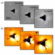 |
| Figure: Infrared visualization of nanocrack evolution. a) Topography of triangular indents (depressions) at the surface of a SiC crystal. Indentation was performed by pressing a sharp diamond tip into the crystal surface. With increasing force F, the depression becomes larger and deeper. b) The infrared near-field images recorded at about 10 �m wavelength clearly show the regions around the indent where the crystal lattice is compressed (bright) or stretched (dark). Because of the exceptional high spatial resolution, the images reveal the onset and formation of nanoscale cracks (marked by dashed blue circlse) when the indentation force is increased. Copyright: Andreas Huber, Max Planck Institute of Biochemistry, Martinsried |
Abstract:
A joint team of researchers at CIC nanoGUNE (San Sebastian, Spain) and the Max Planck Institutes of Biochemistry and Plasma Physics (Munich, Germany) report the non-invasive and nanoscale resolved infrared mapping of strain fields in semiconductors. The method, which is based on near-field microscopy, opens new avenues for analyzing mechanical properties of high-performance materials or for contact-free mapping of local conductivity in strain-engineered electronic devices (Nature Nanotechnology, advanced online publication, 11 Jan. 2009).
Infrared light visualizes nanoscale strain fields
Germany | Posted on January 15th, 2009Visualizing strain at length scales below 100 nm is a key requirement in modern metrology because strain determines the mechanical and electrical properties of high-performance ceramics or modern electronic devices, respectively. The non-invasive mapping of strain with nanoscale spatial resolution, however, is still a challenge.
A promising route for highly sensitive and non-invasive mapping of nanoscale material properties is scattering-type Scanning Near-field Optical Microscopy (s-SNOM). Part of the team had pioneered this technique over the last decade, enabling chemical recognition of nanostructures and mapping of local conductivity in industrial semiconductor nanodevices. The technique makes use of extreme light concentration at the sharp tip of an Atomic Force Microscope (AFM), yielding nanoscale resolved images at visible, infrared and terahertz frequencies. The s-SNOM thus breaks the diffraction barrier throughout the electromagnetic spectrum and with its 20 nm resolving power matches the needs of modern nanoscience and technology.
Now, the research team has provided first experimental evidence that the microscopy technique is capable of mapping local strain and cracks of nanoscale dimensions. This was demonstrated by pressing a sharp diamond tip into the surface of a Silicon Carbide crystal. With the near-field microscope the researchers were able to visualize the nanoscopic strain field around the depression and the generation of nanocracks (see Figure). "Compared to other methods such as electron microscopy, our technique offers the advantage of non-invasive imaging without the need of special sample preparation" says Andreas Huber who performed the experiments within his Ph.D. project. "Specific applications of technological interest could be the detection of nanocracks before they reach critical dimensions, e.g. in ceramics or Micro-Electro-Mechanical Systems (MEMS), and the study of crack propagation", says Alexander Ziegler.
The researchers also demonstrated that s-SNOM offers the intriguing possibility of mapping free-carrier properties such as density and mobility in strained silicon. By controlled straining of silicon, the properties of the free carriers can be designed, which is essential to further shrink and speed-up future computer chips. For both development and quality control, the quantitative and reliable mapping of the carrier mobility is strongly demanded but hitherto no tool has been available. "Our results thus promise interesting applications of s-SNOM in semiconductor science and technology such as the quantitative analysis of the local carrier properties in strain-engineered electronic nanodevices" says Rainer Hillenbrand, leader of the Nano-Photonics Group at MPI and the Nanooptics Laboratory at nanoGUNE.
Original publication:
A. J. Huber, A. Ziegler, T. K�ck, and R. Hillenbrand, Infrared nanoscopy of strained semiconductors, Nat. Nanotech., advanced online publication, 11. Jan. 2009, DOI 10.1038/NNANO.2008.399.
####
For more information, please click here
Contacts:
Dr. Rainer Hillenbrand
Nanooptics Laboratory
CIC nanoGUNE Consolider
20009 Donostia - San Sebastian, Spain
phone: +34 943 574 007
and
Nano-Photonics Group
Max-Planck-Institut f�r Biochemie
82152 Martinsried, Germany
Copyright © Max-Planck-Institut f�r Biochemie
If you have a comment, please Contact us.Issuers of news releases, not 7th Wave, Inc. or Nanotechnology Now, are solely responsible for the accuracy of the content.
Bookmark:


| Related News Press |
News and information
![]() Quantum computer improves AI predictions April 17th, 2026
Quantum computer improves AI predictions April 17th, 2026
![]() Flexible sensor gains sensitivity under pressure April 17th, 2026
Flexible sensor gains sensitivity under pressure April 17th, 2026
![]() A reusable chip for particulate matter sensing April 17th, 2026
A reusable chip for particulate matter sensing April 17th, 2026
![]() Detecting vibrational quantum beating in the predissociation dynamics of SF6 using time-resolved photoelectron spectroscopy April 17th, 2026
Detecting vibrational quantum beating in the predissociation dynamics of SF6 using time-resolved photoelectron spectroscopy April 17th, 2026
Imaging
![]() Simple algorithm paired with standard imaging tool could predict failure in lithium metal batteries August 8th, 2025
Simple algorithm paired with standard imaging tool could predict failure in lithium metal batteries August 8th, 2025
Chip Technology
![]() A reusable chip for particulate matter sensing April 17th, 2026
A reusable chip for particulate matter sensing April 17th, 2026
![]() Metasurfaces smooth light to boost magnetic sensing precision January 30th, 2026
Metasurfaces smooth light to boost magnetic sensing precision January 30th, 2026
Discoveries
![]() Quantum computer improves AI predictions April 17th, 2026
Quantum computer improves AI predictions April 17th, 2026
![]() Flexible sensor gains sensitivity under pressure April 17th, 2026
Flexible sensor gains sensitivity under pressure April 17th, 2026
![]() A reusable chip for particulate matter sensing April 17th, 2026
A reusable chip for particulate matter sensing April 17th, 2026
![]() Detecting vibrational quantum beating in the predissociation dynamics of SF6 using time-resolved photoelectron spectroscopy April 17th, 2026
Detecting vibrational quantum beating in the predissociation dynamics of SF6 using time-resolved photoelectron spectroscopy April 17th, 2026
Announcements
![]() A fundamentally new therapeutic approach to cystic fibrosis: Nanobody repairs cellular defect April 17th, 2026
A fundamentally new therapeutic approach to cystic fibrosis: Nanobody repairs cellular defect April 17th, 2026
![]() UC Irvine physicists discover method to reverse �quantum scrambling� : The work addresses the problem of information loss in quantum computing system April 17th, 2026
UC Irvine physicists discover method to reverse �quantum scrambling� : The work addresses the problem of information loss in quantum computing system April 17th, 2026
|
|
||
|
|
||
| The latest news from around the world, FREE | ||
|
|
||
|
|
||
| Premium Products | ||
|
|
||
|
Only the news you want to read!
Learn More |
||
|
|
||
|
Full-service, expert consulting
Learn More |
||
|
|
||