Home > Press > On the Boil: New Nano Technique Significantly Boosts Boiling Efficiency
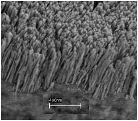 |
| A scanning electron microscope shows copper nanorods deposited on a copper substrate. Air trapped in the forest of nanorods helps to dramatically boost the creation of bubbles and the efficiency of boiling, which in turn could lead to new ways of cooling computer chips as well as cost savings for any number of industrial boiling application.
Photo Credit: Rensselaer/Koratkar |
Abstract:
Hyper-efficient boiling could lead to smaller computer chips, lower energy costs
On the Boil: New Nano Technique Significantly Boosts Boiling Efficiency
Troy, NY | Posted on July 2nd, 2008Whoever penned the old adage "a watched pot never boils" surely never tried to heat up water in a pot lined with copper nanorods.
A new study from researchers at Rensselaer Polytechnic Institute shows that by adding an invisible layer of the nanomaterials to the bottom of a metal vessel, an order of magnitude less energy is required to bring water to boil. This increase in efficiency could have a big impact on cooling computer chips, improving heat transfer systems, and reducing costs for industrial boiling applications.
"Like so many other nanotechnology and nanomaterials breakthroughs, our discovery was completely unexpected," said Nikhil A. Koratkar, associate professor in the Department of Mechanical, Aerospace, and Nuclear Engineering at Rensselaer, who led the project. "The increased boiling efficiency seems to be the result of an interesting interplay between the nanoscale and microscale surfaces of the treated metal. The potential applications for this discovery are vast and exciting, and we're eager to continue our investigations into this phenomenon."
Bringing water to a boil, and the related phase change that transforms the liquid into vapor, requires an interface between the water and air. In the example of a pot of water, two such interfaces exist: at the top where the water meets air, and at the bottom where the water meets tiny pockets of air trapped in the microscale texture and imperfections on the surface of the pot. Even though most of the water inside of the pot has reached 100 degrees Celsius and is at boiling temperature, it cannot boil because it is surrounded by other water molecules and there is no interface � i.e., no air � present to facilitate a phase change.
Bubbles are typically formed when air is trapped inside a microscale cavity on the metal surface of a vessel, and vapor pressure forces the bubble to the top of the vessel. As this bubble nucleation takes place, water floods the microscale cavity, which in turn prevents any further nucleation from occurring at that specific site.
Koratkar and his team found that by depositing a layer of copper nanorods on the surface of a copper vessel, the nanoscale pockets of air trapped within the forest of nanorods "feed" nanobubbles into the microscale cavities of the vessel surface and help to prevent them from getting flooded with water. This synergistic coupling effect promotes robust boiling and stable bubble nucleation, with large numbers of tiny, frequently occurring bubbles.
"By themselves, the nanoscale and microscale textures are not able to facilitate good boiling, as the nanoscale pockets are simply too small and the microscale cavities are quickly flooded by water and therefore single-use," Koratkar said. "But working together, the multiscale effect allows for significantly improved boiling. We observed a 30-fold increase in active bubble nucleation site density � a fancy term for the number of bubbles created � on the surface treated with copper nanotubes, over the nontreated surface."
Boiling is ultimately a vehicle for heat transfer, in that it moves energy from a heat source to the bottom of a vessel and into the contained liquid, which then boils, and turns into vapor that eventually releases the heat into the atmosphere. This new discovery allows this process to become significantly more efficient, which could translate into considerable efficiency gains and cost savings if incorporated into a wide range of industrial equipment that relies on boiling to create heat or steam.
"If the amount of energy it takes to boil water is reduced by an order of magnitude, that should translate into significant cost savings," he said.
The team's discovery could also revolutionize the process of cooling computer chips. As the physical size of chips has shrunk significantly over the past two decades, it has become increasingly critical to develop ways to cool hot spots and transfer lingering heat away from the chip. This challenge has grown more prevalent in recent years, and threatens to bottleneck the semiconductor industry's ability to develop smaller and more powerful chips.
Boiling is a potential heat transfer technique that can be used to cool chips, Koratkar said, so depositing copper nanorods onto the copper interconnects of chips could lead to new innovations in heat transfer and dissipation for semiconductors.
"Since computer interconnects are already made of copper, it should be easy and inexpensive to treat those components with a layer of copper nanorods," Koratkar said, noting that his group plans to further pursue this possibility.
The research results of Koratkar's study are presented in the paper "Nanostructure copper interfaces for enhanced boiling," which was published online this week and will appear in a forthcoming issue of the journal Small.
The study may be accessed online at: www3.interscience.wiley.com/journal/120081321/abstract
Along with Koratkar, co-authors of the paper include Rensselaer MANE Associate Professor Yoav Peles; Rensselaer mechanical engineering graduate student Zuankai Wang; Rensselaer Center for Integrated Electronics Research Associate Pei-I Wang; University of Colorado at Boulder Chancellor and former Rensselaer Provost G.P. "Bud" Peterson; and UC-Boulder Assistant Research Professor Chen Li.
The research was funded by the National Science Foundation.
####
About Rensselaer Polytechnic Institute
Rensselaer Polytechnic Institute, founded in 1824, is the nation�s oldest technological university. The university offers bachelor�s, master�s, and doctoral degrees in engineering, the sciences, information technology, architecture, management, and the humanities and social sciences. Institute programs serve undergraduates, graduate students, and working professionals around the world. Rensselaer faculty are known for pre-eminence in research conducted in a wide range of fields, with particular emphasis in biotechnology, nanotechnology, information technology, and the media arts and technology. The Institute is well known for its success in the transfer of technology from the laboratory to the marketplace so that new discoveries and inventions benefit human life, protect the environment, and strengthen economic development.
For more information, please click here
Contacts:
Michael Mullaney
Phone: (518) 276-6161
Copyright © Rensselaer Polytechnic Institute
If you have a comment, please Contact us.Issuers of news releases, not 7th Wave, Inc. or Nanotechnology Now, are solely responsible for the accuracy of the content.
Bookmark:


| Related News Press |
News and information
![]() Simulating magnetization in a Heisenberg quantum spin chain April 5th, 2024
Simulating magnetization in a Heisenberg quantum spin chain April 5th, 2024
![]() NRL charters Navy�s quantum inertial navigation path to reduce drift April 5th, 2024
NRL charters Navy�s quantum inertial navigation path to reduce drift April 5th, 2024
![]() Discovery points path to flash-like memory for storing qubits: Rice find could hasten development of nonvolatile quantum memory April 5th, 2024
Discovery points path to flash-like memory for storing qubits: Rice find could hasten development of nonvolatile quantum memory April 5th, 2024
Govt.-Legislation/Regulation/Funding/Policy
![]() NRL charters Navy�s quantum inertial navigation path to reduce drift April 5th, 2024
NRL charters Navy�s quantum inertial navigation path to reduce drift April 5th, 2024
![]() Discovery points path to flash-like memory for storing qubits: Rice find could hasten development of nonvolatile quantum memory April 5th, 2024
Discovery points path to flash-like memory for storing qubits: Rice find could hasten development of nonvolatile quantum memory April 5th, 2024
![]() Chemical reactions can scramble quantum information as well as black holes April 5th, 2024
Chemical reactions can scramble quantum information as well as black holes April 5th, 2024
Academic/Education
![]() Rice University launches Rice Synthetic Biology Institute to improve lives January 12th, 2024
Rice University launches Rice Synthetic Biology Institute to improve lives January 12th, 2024
![]() Multi-institution, $4.6 million NSF grant to fund nanotechnology training September 9th, 2022
Multi-institution, $4.6 million NSF grant to fund nanotechnology training September 9th, 2022
Chip Technology
![]() Discovery points path to flash-like memory for storing qubits: Rice find could hasten development of nonvolatile quantum memory April 5th, 2024
Discovery points path to flash-like memory for storing qubits: Rice find could hasten development of nonvolatile quantum memory April 5th, 2024
![]() Utilizing palladium for addressing contact issues of buried oxide thin film transistors April 5th, 2024
Utilizing palladium for addressing contact issues of buried oxide thin film transistors April 5th, 2024
![]() HKUST researchers develop new integration technique for efficient coupling of III-V and silicon February 16th, 2024
HKUST researchers develop new integration technique for efficient coupling of III-V and silicon February 16th, 2024
Discoveries
![]() Chemical reactions can scramble quantum information as well as black holes April 5th, 2024
Chemical reactions can scramble quantum information as well as black holes April 5th, 2024
![]() New micromaterial releases nanoparticles that selectively destroy cancer cells April 5th, 2024
New micromaterial releases nanoparticles that selectively destroy cancer cells April 5th, 2024
![]() Utilizing palladium for addressing contact issues of buried oxide thin film transistors April 5th, 2024
Utilizing palladium for addressing contact issues of buried oxide thin film transistors April 5th, 2024
Announcements
![]() NRL charters Navy�s quantum inertial navigation path to reduce drift April 5th, 2024
NRL charters Navy�s quantum inertial navigation path to reduce drift April 5th, 2024
![]() Discovery points path to flash-like memory for storing qubits: Rice find could hasten development of nonvolatile quantum memory April 5th, 2024
Discovery points path to flash-like memory for storing qubits: Rice find could hasten development of nonvolatile quantum memory April 5th, 2024
Energy
![]() Development of zinc oxide nanopagoda array photoelectrode: photoelectrochemical water-splitting hydrogen production January 12th, 2024
Development of zinc oxide nanopagoda array photoelectrode: photoelectrochemical water-splitting hydrogen production January 12th, 2024
![]() Shedding light on unique conduction mechanisms in a new type of perovskite oxide November 17th, 2023
Shedding light on unique conduction mechanisms in a new type of perovskite oxide November 17th, 2023
![]() Inverted perovskite solar cell breaks 25% efficiency record: Researchers improve cell efficiency using a combination of molecules to address different November 17th, 2023
Inverted perovskite solar cell breaks 25% efficiency record: Researchers improve cell efficiency using a combination of molecules to address different November 17th, 2023
![]() The efficient perovskite cells with a structured anti-reflective layer � another step towards commercialization on a wider scale October 6th, 2023
The efficient perovskite cells with a structured anti-reflective layer � another step towards commercialization on a wider scale October 6th, 2023
|
|
||
|
|
||
| The latest news from around the world, FREE | ||
|
|
||
|
|
||
| Premium Products | ||
|
|
||
|
Only the news you want to read!
Learn More |
||
|
|
||
|
Full-service, expert consulting
Learn More |
||
|
|
||