Home > Press > IP Profile: Lightanate: Photocatalysts for Harnessing Visible Light
 |
| Lightanate Image, Courtesy of Fouad Haghseresht, UniQuest, Australia |
Abstract:
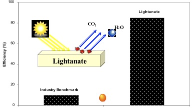
Lightanate can make the use of photocatalytic processes in water treatment affordable. Since existing photocatalysts are ultra violet light activated, by being able to use visible light, Lightanate technology has the potential of harnessing up to nine times more available energy than the existing photocatalysts.
IP Profile: Lightanate: Photocatalysts for Harnessing Visible Light
Boston, MA | Posted on May 22nd, 2008Organization: Australian Research Council Centre of Excellence for Functional Nanomaterials, University of Queensland, Australia
Industry Market: Energy
Technology Contact: F. Haghseresht, UniQuest, Australia
Lightanate is a technology which uses photocatalysts to harness the energy of visible light. It was developed at the Australian Research Council Centre of excellence for Functional Nanomaterials, University of Queensland, Australia.
Photocatalysts speed up chemical reactions when exposed to light. They are recyclable, potentially renewable, non-toxic and versatile. They can be used in a range of applications, including, water treatment and air purification. The uses of photocatalytic processes in these applications are known to deliver significant environmental benefits, without creating harmful by-products.
Lightanate can make the use of photocatalytic processes in water treatment affordable. Since existing photocatalysts are ultra violet light activated, by being able to use visible light, Lightanate technology has the potential of harnessing up to nine times more available energy than the existing photocatalysts. As a result, of this advantage, the capital and operational costs of Lightanate-based photocatalytic process are expected to be significantly less than those that use currently available photocatalysts.
Lightanate technology will be licensed to a start-up company of the same name to attract investment for commercialising this technology in water treatment. Last year, Lightanate was a finalist in UQ Business School's prestigious $100,000 Enterprize business plan competition.
We are currently engaging with industry, seeking regulatory approvals, and subject to finalising an investment deal; we plan to commence manufacturing trials for the Lightanate technology within 12 months.
####
About NSTI
The Nano Science and Technology Institute (NSTI) is chartered with the promotion and integration of nano and other advanced technologies through education, technology and business development. NSTI accomplishes this mission through its offerings of continuing education programs, scientific and business publishing and community outreach. NSTI produces the annual Nanotech conference and trade show, the most comprehensive international nanotechnology convention in the world. NSTI also produces the semi-annual Nanotech Venture, Nanotech Industrial Impact Workshop, Nano Impact Summit and the Nanotech Course Series in the US and Europe. NSTI was founded in 1997 as a result of the merger between various scientific societies, and is headquartered in Cambridge, Massachusetts with additional offices in California and Switzerland.
For more information, please click here
Contacts:
Sarah Wenning
696 San Ramon Valley Blvd., Ste. 423
Danville, CA 94526
Ph: (925) 901-4959
Fax: (925) 886-8461
Copyright © NSTI
If you have a comment, please Contact us.Issuers of news releases, not 7th Wave, Inc. or Nanotechnology Now, are solely responsible for the accuracy of the content.
Bookmark:


| Related News Press |
News and information
![]() Simulating magnetization in a Heisenberg quantum spin chain April 5th, 2024
Simulating magnetization in a Heisenberg quantum spin chain April 5th, 2024
![]() NRL charters Navy�s quantum inertial navigation path to reduce drift April 5th, 2024
NRL charters Navy�s quantum inertial navigation path to reduce drift April 5th, 2024
![]() Discovery points path to flash-like memory for storing qubits: Rice find could hasten development of nonvolatile quantum memory April 5th, 2024
Discovery points path to flash-like memory for storing qubits: Rice find could hasten development of nonvolatile quantum memory April 5th, 2024
Announcements
![]() NRL charters Navy�s quantum inertial navigation path to reduce drift April 5th, 2024
NRL charters Navy�s quantum inertial navigation path to reduce drift April 5th, 2024
![]() Discovery points path to flash-like memory for storing qubits: Rice find could hasten development of nonvolatile quantum memory April 5th, 2024
Discovery points path to flash-like memory for storing qubits: Rice find could hasten development of nonvolatile quantum memory April 5th, 2024
Energy
![]() Development of zinc oxide nanopagoda array photoelectrode: photoelectrochemical water-splitting hydrogen production January 12th, 2024
Development of zinc oxide nanopagoda array photoelectrode: photoelectrochemical water-splitting hydrogen production January 12th, 2024
![]() Shedding light on unique conduction mechanisms in a new type of perovskite oxide November 17th, 2023
Shedding light on unique conduction mechanisms in a new type of perovskite oxide November 17th, 2023
![]() Inverted perovskite solar cell breaks 25% efficiency record: Researchers improve cell efficiency using a combination of molecules to address different November 17th, 2023
Inverted perovskite solar cell breaks 25% efficiency record: Researchers improve cell efficiency using a combination of molecules to address different November 17th, 2023
![]() The efficient perovskite cells with a structured anti-reflective layer � another step towards commercialization on a wider scale October 6th, 2023
The efficient perovskite cells with a structured anti-reflective layer � another step towards commercialization on a wider scale October 6th, 2023
Events/Classes
![]() Researchers demonstrate co-propagation of quantum and classical signals: Study shows that quantum encryption can be implemented in existing fiber networks January 20th, 2023
Researchers demonstrate co-propagation of quantum and classical signals: Study shows that quantum encryption can be implemented in existing fiber networks January 20th, 2023
Solar/Photovoltaic
![]() Development of zinc oxide nanopagoda array photoelectrode: photoelectrochemical water-splitting hydrogen production January 12th, 2024
Development of zinc oxide nanopagoda array photoelectrode: photoelectrochemical water-splitting hydrogen production January 12th, 2024
![]() Shedding light on unique conduction mechanisms in a new type of perovskite oxide November 17th, 2023
Shedding light on unique conduction mechanisms in a new type of perovskite oxide November 17th, 2023
![]() Inverted perovskite solar cell breaks 25% efficiency record: Researchers improve cell efficiency using a combination of molecules to address different November 17th, 2023
Inverted perovskite solar cell breaks 25% efficiency record: Researchers improve cell efficiency using a combination of molecules to address different November 17th, 2023
![]() Charged �molecular beasts� the basis for new compounds: Researchers at Leipzig University use �aggressive� fragments of molecular ions for chemical synthesis November 3rd, 2023
Charged �molecular beasts� the basis for new compounds: Researchers at Leipzig University use �aggressive� fragments of molecular ions for chemical synthesis November 3rd, 2023
|
|
||
|
|
||
| The latest news from around the world, FREE | ||
|
|
||
|
|
||
| Premium Products | ||
|
|
||
|
Only the news you want to read!
Learn More |
||
|
|
||
|
Full-service, expert consulting
Learn More |
||
|
|
||