Home > Press > New Polymer Could Improve Semiconductor Manufacturing, Packaging
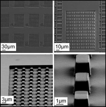 |
| Researchers in Rensselaer�s Department of Physics and Center for Integrated Electronics have developed a new inexpensive, quick-drying polymer that could lead to dramatic cost savings and efficiency gains in semiconductor manufacturing and computer chip packaging. In this scanning electron microscope image of PES in a UV-imprint lithography application, the well-defined pattern indicates the material�s potential for use in next-generation chip making techniques. |
Abstract:
Researchers at Rensselaer Polytechnic Institute and Polyset Company have developed a new inexpensive, quick-drying polymer that could lead to dramatic cost savings and efficiency gains in semiconductor manufacturing and computer chip packaging.
New Polymer Could Improve Semiconductor Manufacturing, Packaging
Troy, NY | Posted on January 29th, 2008Along with allowing enhanced performance and cost savings for conventional photolithography processes, the new material, called polyset epoxy siloxane (PES), should also enable a new generation of lower-cost, on-chip nanoimprinting lithography technology, according to the researchers.
"With this new material, chip manufacturers will be able to trim several steps from their production and packaging processes, and in turn realize a cost savings," said Toh-Ming Lu, the R.P. Baker Distinguished Professor of Physics at Rensselaer, who oversaw the study. "PES is cheaper and more reliable."
Lu's research was published this week in the Journal of Vacuum Science and Technology B.
The widely adopted technique of photolithography involves using a mix of light and chemicals to generate intricate micro- and nano-scale patterns on tiny areas of silicon. As part of the process, a thin polymer film � called a redistribution layer, and crucial to the effectiveness of device � is deposited onto the silicon wafer, in order to ease the signal propagation delay and to protect the chip from different environmental and mechanical factors.
The new PES material developed by Lu's group and Polyset Company is one such thin polymer film, and it offers several advantages over the incumbent materials typically used in the semiconductor manufacturing industry. In addition, their new PES material can also be used as a thin polymer film for ultraviolet (UV) on-chip nanoimprinting lithography technology, which is still in the early phases of development. The consistency of using PES in conventional technology, and then continuing to use PES while academia and industry test and gradually migrate to the next generation of devices, should help ease the transition, Lu said.
"Having the ability to use one material � our new PES � for both photolithography and imprint will be very attractive to manufacturers," Lu said. "At its core, our project is basic research, but it also has important industry implications. It's very exciting."
Manufacturers today typically use benzocyclobutene and polyimide as polymers for redistribution layers, because of their low water absorption, thermal stability, low curing temperature, low thermal expansion, low dielectric constant, and low leakage current. Lu said PES offers significant advantages to these materials, particularly in the areas of cure temperature and water uptake.
PES cures, or dries and hardens, at 165 degrees Celsius, about 35 percent cooler than the other two materials. The need for less heat should translate directly into lower overhead costs for manufacturers, Lu said. Another advantage of PES is its low water uptake rate of less than 0.2 percent, less than the other materials. Additionally, PES adheres well to copper and can easily be made less brittle if needed. All of these attributes make PES a promising candidate for redistribution layer application and UV imprint lithography.
"The results demonstrate that PES is feasible to be used as UV-curable resist for both the redistribution application for electronic packaging and micro/nano imprint lithography," said Rensselaer Research Associate Pei-I Wang, co-author of the paper.
Along with photolithography and on-chip nanoimprinting lithography, PES holds the potential for applications in other optical devices, flat-panel display, biotechnology devices, and microelectromechanical systems, Wang said.
In addition to Lu and Wang, co-authors on the paper include Rensselaer materials science and engineering professor Omkaram Nalamasu, who is also chief technical officer of Applied Materials Inc. in Santa Clara, Calif.; Rajat Ghoshal and Ram Ghoshal of Polyset Co. Inc. in Mechanicville, N.Y.; Charles Schaper of Transfer Devices Inc. in Santa Clara, Calif.; and Andrew Li of Applied Materials.
The project was funded through the New York State Foundation for Science, Technology and Innovation.
Lu's research was conducted as part of Rensselaer's Center for Integrated Electronics. The center's multidisciplinary team of more than 50 faculty researchers and 100 graduate students aims to advance the role of electronic devices of our everyday lives by accelerating the production of the next generation of micro- and nanoelectronic devices and systems. The Center's mission is to build integrated top-down and bottom-up nanostructures, devices, and systems for information, biological, and broadband communication applications. Major activities include pioneering research into gigascale interconnects, 3-D interconnect structures, materials properties and process modeling, wideband gap semiconductors and devices, terahertz devices and imaging systems, power electronic devices and systems, and biochips.
For more information on Lu's research and Rensselaer's Center for Integrated Electronics, visit: www.rpi.edu/~lut/ and www.rpi.edu/dept/cie.
For more information on the new PES materials, visit: www.polyset.com.
About Rensselaer
####
About Rensselaer Polytechnic Institute
Rensselaer Polytechnic Institute, founded in 1824, is the nation�s oldest technological university. The university offers bachelor�s, master�s, and doctoral degrees in engineering, the sciences, information technology, architecture, management, and the humanities and social sciences. Institute programs serve undergraduates, graduate students, and working professionals around the world. Rensselaer faculty are known for pre-eminence in research conducted in a wide range of fields, with particular emphasis in biotechnology, nanotechnology, information technology, and the media arts and technology. The Institute is well known for its success in the transfer of technology from the laboratory to the marketplace so that new discoveries and inventions benefit human life, protect the environment, and strengthen economic development.
For more information, please click here
Contacts:
Michael Mullaney
Phone: (518) 276-6161
E-mail:
Copyright © Rensselaer Polytechnic Institute
If you have a comment, please Contact us.Issuers of news releases, not 7th Wave, Inc. or Nanotechnology Now, are solely responsible for the accuracy of the content.
Bookmark:


| Related News Press |
News and information
![]() Simulating magnetization in a Heisenberg quantum spin chain April 5th, 2024
Simulating magnetization in a Heisenberg quantum spin chain April 5th, 2024
![]() NRL charters Navy�s quantum inertial navigation path to reduce drift April 5th, 2024
NRL charters Navy�s quantum inertial navigation path to reduce drift April 5th, 2024
![]() Discovery points path to flash-like memory for storing qubits: Rice find could hasten development of nonvolatile quantum memory April 5th, 2024
Discovery points path to flash-like memory for storing qubits: Rice find could hasten development of nonvolatile quantum memory April 5th, 2024
Chip Technology
![]() Discovery points path to flash-like memory for storing qubits: Rice find could hasten development of nonvolatile quantum memory April 5th, 2024
Discovery points path to flash-like memory for storing qubits: Rice find could hasten development of nonvolatile quantum memory April 5th, 2024
![]() Utilizing palladium for addressing contact issues of buried oxide thin film transistors April 5th, 2024
Utilizing palladium for addressing contact issues of buried oxide thin film transistors April 5th, 2024
![]() HKUST researchers develop new integration technique for efficient coupling of III-V and silicon February 16th, 2024
HKUST researchers develop new integration technique for efficient coupling of III-V and silicon February 16th, 2024
Discoveries
![]() Chemical reactions can scramble quantum information as well as black holes April 5th, 2024
Chemical reactions can scramble quantum information as well as black holes April 5th, 2024
![]() New micromaterial releases nanoparticles that selectively destroy cancer cells April 5th, 2024
New micromaterial releases nanoparticles that selectively destroy cancer cells April 5th, 2024
![]() Utilizing palladium for addressing contact issues of buried oxide thin film transistors April 5th, 2024
Utilizing palladium for addressing contact issues of buried oxide thin film transistors April 5th, 2024
Announcements
![]() NRL charters Navy�s quantum inertial navigation path to reduce drift April 5th, 2024
NRL charters Navy�s quantum inertial navigation path to reduce drift April 5th, 2024
![]() Discovery points path to flash-like memory for storing qubits: Rice find could hasten development of nonvolatile quantum memory April 5th, 2024
Discovery points path to flash-like memory for storing qubits: Rice find could hasten development of nonvolatile quantum memory April 5th, 2024
|
|
||
|
|
||
| The latest news from around the world, FREE | ||
|
|
||
|
|
||
| Premium Products | ||
|
|
||
|
Only the news you want to read!
Learn More |
||
|
|
||
|
Full-service, expert consulting
Learn More |
||
|
|
||