Home > Press > Hybrid semiconductors show zero thermal expansion; could lead to hardier electronics and optoelectronics
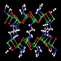 |
| The crystal structure of -ZnTe(en)0:5, determined by single-crystal X-ray diffraction. Two-monolayerthick ZnTe slabs are interconnected by ethylenediamine (C2N2H8) molecules bonded to zinc atoms. Zn-Green, Te-Red, N-Blue,and C-Gray. Hydrogen atoms are omitted for clarity. |
Abstract:
The fan in your computer is there to keep the microprocessor chip from heating to the point where its component materials start to expand, inducing cracks that interrupt the flow of electricity — and not incidentally, ruin the chip. Thermal expansion can also separate semiconducting materials from the substrate, reduce performance through changes in the electronic structure of the material or warp the delicate structures that emit laser light.
Hybrid semiconductors show zero thermal expansion; could lead to hardier electronics and optoelectronics
ARGONNE, IL | Posted on December 19th, 2007Recently published research by scientists at the U.S. Department of Energy's National Renewable Energy Laboratory (NREL) and Argonne National Laboratory, and academic institutions has shed light on a semiconducting material with zero thermal expansion (ZTE). The research may play a role in the design of future generations of electronics and optoelectronics that can withstand a wide range of temperatures.
Traditional interests in ZTE materials have largely been in areas such as optics, heat-engine components and kitchenware. ZTE materials with applications in non-conventional areas such as electronics and optoelectronics are rare; most are glasses, which do not work well in electronics applications. The hybrid inorganic-organic semiconductor investigated in this work is a multifunctional semiconductor that has previously been shown to possess superior electronic and optical properties. The work also suggests an alternative route to designing materials with any desired positive or negative thermal expansion.
"It's a merger of inorganic and organic materials," said Zahirul Islam, a physicist in Argonne's X-Ray Science Division, "which form a fully coherent, three-dimensionally ordered crystal. Normally inorganic and organic materials don't work very well together, but here they are working together to display these remarkable properties."
The materials under study form alternating organic and inorganic layers that work together to produce these effects. One contracts while the other expands, and the net effect is zero.
"This work suggests a novel approach to design the thermal expansion — from positive to negative, including zero — in a nanoscopic scale by assembling nano-scale units in an ordered manner," said principal investigator Yong Zhang of NREL. "The idea has only been demonstrated for tuning thermal expansion in one dimension and study was limited to one or two materials. Next, we would like to extend the idea to higher dimensions (i.e., ZTE in more than one dimension), and explore more inorganic-organic combinations."
These hybrid materials hold promise for high-efficiency semiconductor lasers, ultrathin and flexible solar cells and light-emitting and detecting devices. It is possible to "dope" the materials (adding small amounts of other compounds) to form transparent conducting materials, Zhang said.
While chemical and thermal stability are two major problems for most hybrids, the hybrid nanostructures investigated in this work are found to be exceptionally stable in the air, even under the illumination of an ultraviolet laser.
"Not only do the crystal structures remain unchanged," Zhang said, "but their electronic and optical properties remain after a few years of air exposure or upon heating to more than 200 degrees C, a feature attributed to the strong covalent bonding throughout the structure."
This work involved multiple institutes with complementary strengths and capabilities. Scientists at NREL initiated and organized the project. The materials were synthesized by Jing Li's group at Rutgers University. Critical X-ray diffraction measurements to determine the ZTE effects were carried out at Argonne's Advanced Photon Source. Other key Argonne researchers are Yang Ren and Peter L. Lee. Theoretical modeling on the phonon (vibrational) spectrum, crucial to the understanding of the experimental findings, was performed by scientists at the University of Arkansas. Collaborators at the University of Colorado at Boulder also made important contributions to the work.
####
About Argonne National Laboratory
Argonne National Laboratory, a renowned R&D center, brings the world's brightest scientists and engineers together to find exciting and creative new solutions to pressing national problems in science and technology. The nation's first national laboratory, Argonne conducts leading-edge basic and applied scientific research in virtually every scientific discipline. Argonne researchers work closely with researchers from hundreds of companies, universities, and federal, state and municipal agencies to help them solve their specific problems, advance America 's scientific leadership and prepare the nation for a better future. With employees from more than 60 nations, Argonne is managed by UChicago Argonne, LLC for the U.S. Department of Energy's Office of Science.
By Dave Jacqué.
For more information, please click here
Contacts:
Steve McGregor
630/252-5580
at Argonne
Copyright © Argonne National Laboratory
If you have a comment, please Contact us.Issuers of news releases, not 7th Wave, Inc. or Nanotechnology Now, are solely responsible for the accuracy of the content.
Bookmark:


| Related News Press |
News and information
![]() Quantum computer improves AI predictions April 17th, 2026
Quantum computer improves AI predictions April 17th, 2026
![]() Flexible sensor gains sensitivity under pressure April 17th, 2026
Flexible sensor gains sensitivity under pressure April 17th, 2026
![]() A reusable chip for particulate matter sensing April 17th, 2026
A reusable chip for particulate matter sensing April 17th, 2026
![]() Detecting vibrational quantum beating in the predissociation dynamics of SF6 using time-resolved photoelectron spectroscopy April 17th, 2026
Detecting vibrational quantum beating in the predissociation dynamics of SF6 using time-resolved photoelectron spectroscopy April 17th, 2026
Laboratories
![]() Researchers develop molecular qubits that communicate at telecom frequencies October 3rd, 2025
Researchers develop molecular qubits that communicate at telecom frequencies October 3rd, 2025
![]() A battery’s hopping ions remember where they’ve been: Seen in atomic detail, the seemingly smooth flow of ions through a battery’s electrolyte is surprisingly complicated February 16th, 2024
A battery’s hopping ions remember where they’ve been: Seen in atomic detail, the seemingly smooth flow of ions through a battery’s electrolyte is surprisingly complicated February 16th, 2024
Chip Technology
![]() A reusable chip for particulate matter sensing April 17th, 2026
A reusable chip for particulate matter sensing April 17th, 2026
![]() Metasurfaces smooth light to boost magnetic sensing precision January 30th, 2026
Metasurfaces smooth light to boost magnetic sensing precision January 30th, 2026
Discoveries
![]() Quantum computer improves AI predictions April 17th, 2026
Quantum computer improves AI predictions April 17th, 2026
![]() Flexible sensor gains sensitivity under pressure April 17th, 2026
Flexible sensor gains sensitivity under pressure April 17th, 2026
![]() A reusable chip for particulate matter sensing April 17th, 2026
A reusable chip for particulate matter sensing April 17th, 2026
![]() Detecting vibrational quantum beating in the predissociation dynamics of SF6 using time-resolved photoelectron spectroscopy April 17th, 2026
Detecting vibrational quantum beating in the predissociation dynamics of SF6 using time-resolved photoelectron spectroscopy April 17th, 2026
Announcements
![]() A fundamentally new therapeutic approach to cystic fibrosis: Nanobody repairs cellular defect April 17th, 2026
A fundamentally new therapeutic approach to cystic fibrosis: Nanobody repairs cellular defect April 17th, 2026
![]() UC Irvine physicists discover method to reverse ‘quantum scrambling’ : The work addresses the problem of information loss in quantum computing system April 17th, 2026
UC Irvine physicists discover method to reverse ‘quantum scrambling’ : The work addresses the problem of information loss in quantum computing system April 17th, 2026
Alliances/Trade associations/Partnerships/Distributorships
![]() Chicago Quantum Exchange welcomes six new partners highlighting quantum technology solutions, from Chicago and beyond September 23rd, 2022
Chicago Quantum Exchange welcomes six new partners highlighting quantum technology solutions, from Chicago and beyond September 23rd, 2022
![]() University of Illinois Chicago joins Brookhaven Lab's Quantum Center June 10th, 2022
University of Illinois Chicago joins Brookhaven Lab's Quantum Center June 10th, 2022
Research partnerships
![]() Lab to industry: InSe wafer-scale breakthrough for future electronics August 8th, 2025
Lab to industry: InSe wafer-scale breakthrough for future electronics August 8th, 2025
![]() HKU physicists uncover hidden order in the quantum world through deconfined quantum critical points April 25th, 2025
HKU physicists uncover hidden order in the quantum world through deconfined quantum critical points April 25th, 2025
|
|
||
|
|
||
| The latest news from around the world, FREE | ||
|
|
||
|
|
||
| Premium Products | ||
|
|
||
|
Only the news you want to read!
Learn More |
||
|
|
||
|
Full-service, expert consulting
Learn More |
||
|
|
||