Home > Press > Applied Materials’ UVision 3 Sets Benchmark for Brightfield Inspection Sensitivity and Productivity
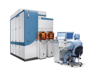 |
| Applied Materials' UVision 3 system delivers 40% faster throughput than any brightfield inspection tool and the 20nm sensitivity needed for advanced immersion lithography. (Photo: Business Wire) |
Abstract:
Applied Materials, Inc. today unveiled its Applied UVision® 3 system, the industry's highest productivity DUV1 Brightfield wafer inspection tool with the critical-defect detection sensitivity required for 45 nanometer (nm) FEOL2 and immersion lithography. Delivering significant advancements to Applied's breakthrough UVision technology, this next-generation system triples the number of laser beams scanning the wafer to provide 40% faster throughput than any competitive system. Two new imaging modes extend sensitivity to 20nm, and a new flexible automatic defect classification engine enables quick access to defects of interest and faster yield learning.
Applied Materials’ UVision 3 Sets Benchmark for Brightfield Inspection Sensitivity and Productivity
SANTA CLARA, CA | Posted on November 26th, 2007 "The UVision 3 system's multi-beam DUV laser architecture allows extendibility beyond the resolution limits of traditional optical inspection," said Dr. Gilad Almogy, vice president and general manager of Applied Materials' Process Diagnostics and Control group. "With this enhanced system, leading-edge memory and immersion lithography manufacturers can run volume production at engineering tool sensitivity with a shorter cycle time to generate meaningful data. We have shipped multiple UVision 3 systems to leading customers where they have validated its exceptional sensitivity at groundbreaking DUV Brightfield throughputs."
By coupling unique laser DUV architecture with a sensitive photo-multiplier tube (PMT) and variable polarization, the UVision 3 system also meets the challenges of 32nm memory development. New Brightfield imaging modes, both in the illumination and collection path, address the contrast versatility required for immersion lithography. In addition, the system's innovative algorithms of high defect accuracy and stitch-to-stitch detection enable enhanced sensitivity on periphery areas, a key advantage not addressed by any other Brightfield system.
UVision 3 is an integral part of Applied Material's advanced lithography-enabling technologies for 45nm and below double patterning and advanced FEOL applications. For more information on the Applied UVision system, visit http://appliedmaterials.com/products/uvision_4.html .
1 DUV=deep ultraviolet
2 FEOL=front end of line
####
About Applied Materials, Inc.
Applied Materials, Inc. (Nasdaq:AMAT) is the global leader in Nanomanufacturing Technology™ solutions with a broad portfolio of innovative equipment, service and software products for the fabrication of semiconductor chips, flat panel displays, solar photovoltaic cells, flexible electronics and energy efficient glass. At Applied Materials, we apply Nanomanufacturing Technology to improve the way people live.
For more information, please click here
Contacts:
Applied Materials, Inc.
Betty Newboe
408-563-0647
(editorial/media)
Randy Bane
408-986-7977
(financial community)
Copyright © Business Wire 2007
If you have a comment, please Contact us.Issuers of news releases, not 7th Wave, Inc. or Nanotechnology Now, are solely responsible for the accuracy of the content.
Bookmark:


| Related News Press |
Chip Technology
![]() A reusable chip for particulate matter sensing April 17th, 2026
A reusable chip for particulate matter sensing April 17th, 2026
![]() Metasurfaces smooth light to boost magnetic sensing precision January 30th, 2026
Metasurfaces smooth light to boost magnetic sensing precision January 30th, 2026
Announcements
![]() A fundamentally new therapeutic approach to cystic fibrosis: Nanobody repairs cellular defect April 17th, 2026
A fundamentally new therapeutic approach to cystic fibrosis: Nanobody repairs cellular defect April 17th, 2026
![]() UC Irvine physicists discover method to reverse ‘quantum scrambling’ : The work addresses the problem of information loss in quantum computing system April 17th, 2026
UC Irvine physicists discover method to reverse ‘quantum scrambling’ : The work addresses the problem of information loss in quantum computing system April 17th, 2026
Tools
![]() Metasurfaces smooth light to boost magnetic sensing precision January 30th, 2026
Metasurfaces smooth light to boost magnetic sensing precision January 30th, 2026
![]() From sensors to smart systems: the rise of AI-driven photonic noses January 30th, 2026
From sensors to smart systems: the rise of AI-driven photonic noses January 30th, 2026
![]() Japan launches fully domestically produced quantum computer: Expo visitors to experience quantum computing firsthand August 8th, 2025
Japan launches fully domestically produced quantum computer: Expo visitors to experience quantum computing firsthand August 8th, 2025
|
|
||
|
|
||
| The latest news from around the world, FREE | ||
|
|
||
|
|
||
| Premium Products | ||
|
|
||
|
Only the news you want to read!
Learn More |
||
|
|
||
|
Full-service, expert consulting
Learn More |
||
|
|
||