Home > Press > Nanomaterials With a Bright Future
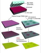 |
| A new fabrication technique, known as soft interference lithography (SIL), makes it possible to inexpensively produce large sheets of gold films with virtually infinite arrays of perforations and microscale "patches" of nanoscale holes. A combination of interference lithography and soft lithography, SIL offers many significant advantages over existing techniques. It can be used to scale-up the nanomanufacturing process to produce plasmonic metamaterials and devices in large quantities. Devices such as films of nanoholes can also serve as templates to make their inverse structures, such as nanoparticles. (Legend: Si=silicon; Cr=chromium; PEEL=electron spectroscopy method called parallel electron energy loss spectroscopy.)
Credit: Reprinted by permission from Macmillan Publishers Ltd: "Multiscale patterning of plasmonic metamaterials," Joel Henzie, Min Hyung Lee and Teri W. Odom, Nature Nanotechnology 2, 549 - 554 (2007) |
Abstract:
New, inexpensive fabrication technique can increase production
Nanomaterials With a Bright Future
Arlington, VA | Posted on September 11th, 2007An innovative and inexpensive way of making nanomaterials on a large scale has resulted in novel forms of advanced materials that pave the way for exceptional and unexpected optical properties. The new fabrication technique, known as soft lithography, or SIL, offers many significant advantages over existing techniques, including the ability to scale-up the manufacturing process to produce devices in large quantities.
The research, funded by the National Science Foundation (NSF) and led by Teri Odom of Northwestern University, appears as the cover story in the September 2007 issue of Nature Nanotechnology.
The optical nanomaterials in this research are called 'plasmonic metamaterials' because their unique physical properties originate from shape and structure rather than material composition only. Two examples of metamaterials in the natural world are peacock feathers and butterfly wings. Their brightly colored patterns are due to structural variations at the hundreds of nanometers level, which cause them to absorb or reflect light.
Through the development of a new nanomanufacturing technique, Odom and her co-workers have succeeded in making gold films with virtually infinite arrays of perforations as small as 100 nanometers--500-1000 times smaller than a human hair. On a magnified scale, these perforated gold films look like Swiss cheese except the perforations are well-ordered and can spread over macroscale distances. The researchers' ability to make these optical metamaterials inexpensively and on large wafers or sheets is what sets this work apart from other techniques.
"One of the biggest problems with nanomaterials has always been their 'scalability,'" Odom said. "It's been very difficult or prohibitively expensive to pattern them over areas larger than about one square millimeter. This research is exciting not only because it demonstrates a new type of patterning technique that is cheap, but also one that can produce very high quality optical materials with interesting properties."
For example, if the perforations or holes are patterned into microscale "patches," they show dramatically different transmission behavior of light compared to an infinite array of holes. The patches appear to focus light while the infinite arrays do not.
Moreover, their optical transmission can be altered simply by changing the geometry of perforations rather than having to "cook" a new composition of materials. This feature makes them very attractive in terms of tuning their behavior to a given need with ease. These materials can also be superior as optical sensors, and they open the possibility of ultra-small sources of light. Furthermore, given their precise organization, they can serve as templates for making their own clones or for making other ordered structures at the nanoscale, such as arrays of nanoparticles.
"This work is exactly the kind of high-risk, high-potential transformative research NSF's Division of Materials Research is interested in supporting," said Harsh Deepak Chopra, NSF program manager. "The early results are extremely promising and suggest a whole new generation of optical devices."
####
About National Science Foundation
he National Science Foundation (NSF) is an independent federal agency that supports fundamental research and education across all fields of science and engineering, with an annual budget of $5.92 billion. NSF funds reach all 50 states through grants to over 1,700 universities and institutions. Each year, NSF receives about 42,000 competitive requests for funding, and makes over 10,000 new funding awards. The NSF also awards over $400 million in professional and service contracts yearly.
For more information, please click here
Contacts:
Diane E. Banegas
NSF
(703) 292-8070
Copyright © National Science Foundation
If you have a comment, please Contact us.Issuers of news releases, not 7th Wave, Inc. or Nanotechnology Now, are solely responsible for the accuracy of the content.
Bookmark:


| Related News Press |
Photonics/Optics/Lasers
![]() With VECSELs towards the quantum internet Fraunhofer: IAF achieves record output power with VECSEL for quantum frequency converters April 5th, 2024
With VECSELs towards the quantum internet Fraunhofer: IAF achieves record output power with VECSEL for quantum frequency converters April 5th, 2024
![]() Nanoscale CL thermometry with lanthanide-doped heavy-metal oxide in TEM March 8th, 2024
Nanoscale CL thermometry with lanthanide-doped heavy-metal oxide in TEM March 8th, 2024
![]() Optically trapped quantum droplets of light can bind together to form macroscopic complexes March 8th, 2024
Optically trapped quantum droplets of light can bind together to form macroscopic complexes March 8th, 2024
![]() HKUST researchers develop new integration technique for efficient coupling of III-V and silicon February 16th, 2024
HKUST researchers develop new integration technique for efficient coupling of III-V and silicon February 16th, 2024
|
|
||
|
|
||
| The latest news from around the world, FREE | ||
|
|
||
|
|
||
| Premium Products | ||
|
|
||
|
Only the news you want to read!
Learn More |
||
|
|
||
|
Full-service, expert consulting
Learn More |
||
|
|
||