Home > Press > Nanoscale Blasting Adjusts Resistance in Magnetic Sensors
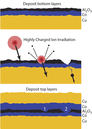 |
| Cartoon illustrates new NIST technique for selectively modifying resistance of a semiconductor device layer. (Top) First layer�in this case a composite of copper and cobalt�and an insulating buffer layer of aluminum oxide is deposited. Buffer is about one nanometer thick. (Middle) Highly charged xenon +44 ions strike the buffer layer, digging nanoscale pits. (Bottom) Top conducting layer of cobalt and copper is deposited. Pits reduce the electrical resistance of the layers and may function as nanoscale GMR sensors embedded in a MTJ sensor.
Credit: NIST |
Abstract:
A new process for adjusting the resistance of semiconductor devices by carpeting a small area of the device with tiny pits, like a yard dug up by demented terriers, may be the key to a new class of magnetic sensors, enabling new, ultra-dense data storage devices. The technique demonstrated by researchers at the National Institute of Standards and Technology (NIST)* allows engineers to tailor the electrical resistance of individual layers in a device without changing any other part of the processing or design.
Nanoscale Blasting Adjusts Resistance in Magnetic Sensors
GAITHERSBURG, MD | Posted on August 16th, 2007The tiny magnetic sensors in modern disk drives are a sandwich of two magnetic layers separated by a thin buffer layer. The layer closest to the disk surface is designed to switch its magnetic polarity quickly in response to the direction of the magnetic "bit" recorded on the disk under it. The sensor works by measuring the electrical resistance across the magnetic layers, which changes depending on whether the two layers have matching polarities.
As manufacturers strive to make disk storage devices smaller and more densely packed with data, the sensors need to shrink as well, but current designs are starting to hit the wall. To meet the size constraints, prototype sensors measure sensor resistance perpendicular to the thin layers, but depending on the buffer material in the sensor, two different types of sensors can be made. Giant magneto-resistance (GMR) sensors use a low-resistance metal buffer layer and are fast, but plagued by very low, difficult to detect, signals. On the other hand, magnetic tunnel junction (MTJ) sensors use a relatively high-resistance insulating buffer that delivers a strong signal, but has a slower response time, too slow to keep up with a very high-speed, high-capacity drive.
What's needed, says NIST physicist Josh Pomeroy, is a compromise. "Our approach is to combine these at the nanometer scale. We start out with a magnetic tunnel junction�an insulating buffer�and then, by using highly charged ions, sort of blow out little craters in the buffer layer so that when we grow the rest of the sensor on top, these craters will act like little GMR sensors, while the rest will act like an MTJ sensor." The combined signal of the two effects, the researchers argue, should be superior to either alone.
The NIST team has demonstrated the first step�the controlled pockmarking of an insulating layer in a multi-layer structure to adjust its total resistance. The team uses small numbers of highly charged xenon ions that each have enormous potential energies�and can blast out surface pits without damaging the substrate. With each ion carrying more than 50 thousand electron volts of potential energy, only one impact is needed to create a pit�multiple hits in the same location are not necessary. Controlling the number of ions provides fine control over the number of pits etched, and hence the resistance of the layer�currently demonstrated over a range of three orders of magnitude. NIST researchers now are working to incorporate these modified layers into working magnetic sensors.
The new technique alters only a single step in the fabrication process�an important consideration for future scale-up�and can be applied to any device where it's desirable to fine-tune the resistance of individual layers. NIST has a provisional patent on the work, number 60,905,125.
* J.M. Pomeroy, H. Grube, A.C. Perrella and J.D. Gillaspy. Selectable resistance-area product by dilute highly charged ion irradiation. Appl. Phys. Lett. 91, 073506 (2007).
####
About NIST
From automated teller machines and atomic clocks to mammograms and semiconductors, innumerable products and services rely in some way on technology, measurement, and standards provided by the National Institute of Standards and Technology.
Founded in 1901, NIST is a non-regulatory federal agency within the U.S. Department of Commerce. NIST's mission is to promote U.S. innovation and industrial competitiveness by advancing measurement science, standards, and technology in ways that enhance economic security and improve our quality of life.
For more information, please click here
Contacts:
Michael Baum
(301) 975-2763
Copyright © NIST
If you have a comment, please Contact us.Issuers of news releases, not 7th Wave, Inc. or Nanotechnology Now, are solely responsible for the accuracy of the content.
Bookmark:


| Related News Press |
Sensors
Discoveries
![]() Chemical reactions can scramble quantum information as well as black holes April 5th, 2024
Chemical reactions can scramble quantum information as well as black holes April 5th, 2024
![]() New micromaterial releases nanoparticles that selectively destroy cancer cells April 5th, 2024
New micromaterial releases nanoparticles that selectively destroy cancer cells April 5th, 2024
![]() Utilizing palladium for addressing contact issues of buried oxide thin film transistors April 5th, 2024
Utilizing palladium for addressing contact issues of buried oxide thin film transistors April 5th, 2024
Announcements
![]() NRL charters Navy�s quantum inertial navigation path to reduce drift April 5th, 2024
NRL charters Navy�s quantum inertial navigation path to reduce drift April 5th, 2024
![]() Discovery points path to flash-like memory for storing qubits: Rice find could hasten development of nonvolatile quantum memory April 5th, 2024
Discovery points path to flash-like memory for storing qubits: Rice find could hasten development of nonvolatile quantum memory April 5th, 2024
Patents/IP/Tech Transfer/Licensing
![]() Getting drugs across the blood-brain barrier using nanoparticles March 3rd, 2023
Getting drugs across the blood-brain barrier using nanoparticles March 3rd, 2023
![]() Metasurfaces control polarized light at will: New research unlocks the hidden potential of metasurfaces August 13th, 2021
Metasurfaces control polarized light at will: New research unlocks the hidden potential of metasurfaces August 13th, 2021
![]() Arrowhead Pharmaceuticals Announces Closing of Agreement with Takeda November 27th, 2020
Arrowhead Pharmaceuticals Announces Closing of Agreement with Takeda November 27th, 2020
|
|
||
|
|
||
| The latest news from around the world, FREE | ||
|
|
||
|
|
||
| Premium Products | ||
|
|
||
|
Only the news you want to read!
Learn More |
||
|
|
||
|
Full-service, expert consulting
Learn More |
||
|
|
||